Flexible MEMS transducer and manufacturing method thereof, and flexible MEMS wireless microphone

a technology of flexible mems and transducers, applied in the direction of electrical transducers, acceleration measurement using interia forces, instruments, etc., can solve the problems of inconvenient use of polymeric materials, polymeric materials deteriorating, and inability to use flexible polymeric materials other than silicon wafers as substrate materials, etc., to achieve enhanced chemical vapor deposition

Inactive Publication Date: 2005-11-22
SAMSUNG ELECTRONICS CO LTD
View PDF1 Cites 65 Cited by
  • Summary
  • Abstract
  • Description
  • Claims
  • Application Information

AI Technical Summary

Benefits of technology

[0011]Therefore, in order to solve at least some of the above-described problems, it is a feature of an embodiment of the present invention to provide a microphone, which has characteristics of softness, flexibility and foldability, by forming a MEMS transducer structure on a flexible polymer substrate using a plasma enhanced chemical vapor deposition (PECVD) process.

Problems solved by technology

The CVD process to form a silicon nitride thin film and a silicon oxide layer on a silicon wafer is a high temperature process requiring a process temperature of about 780 to 850° C. Therefore, it is impossible to use a flexible polymeric material other than the silicon wafer as a material for the substrate.
Thus, when polymeric materials are subjected to a process for forming a thin film at a high temperature, the polymeric materials deteriorate.
Therefore, polymeric materials are not suitable for use as a material for the substrate, such as a wafer, in a process for manufacturing MEMS, which requires a process temperature that is higher than melting points of the polymeric materials.
In practice, silicon MEMS and semiconductors, which are widely used and have excellent characteristics in terms of performance and degree of integration, are generally produced by methods including a high temperature process of at least 500° C. Therefore, the substrate of a high molecular (polymeric) material, which is needed for a flexible system structure, cannot be used.
However, since a very high temperature is needed to form a high-utility thin film by CVD, a low-melting point substrate, such as a polymer, glass, or the like, cannot be used.
However, this method has disadvantages in that the conventional MEMS process, which includes a high temperature process, is used and a polymer process is additionally performed in a final step, thereby increasing the complexity and the cost of the entire manufacturing process.

Method used


Image

  • Flexible MEMS transducer and manufacturing method thereof, and flexible MEMS wireless microphone
  • Flexible MEMS transducer and manufacturing method thereof, and flexible MEMS wireless microphone
  • Flexible MEMS transducer and manufacturing method thereof, and flexible MEMS wireless microphone

Examples


Embodiment Construction

[0043]Korean Patent Application No. 2002-58313, filed on Sep. 26, 2002, and entitled: “Flexible MEMS Transducer and its Manufacturing Method, and Flexible MEMS Wireless Microphone,” is incorporated by reference herein in its entirety.

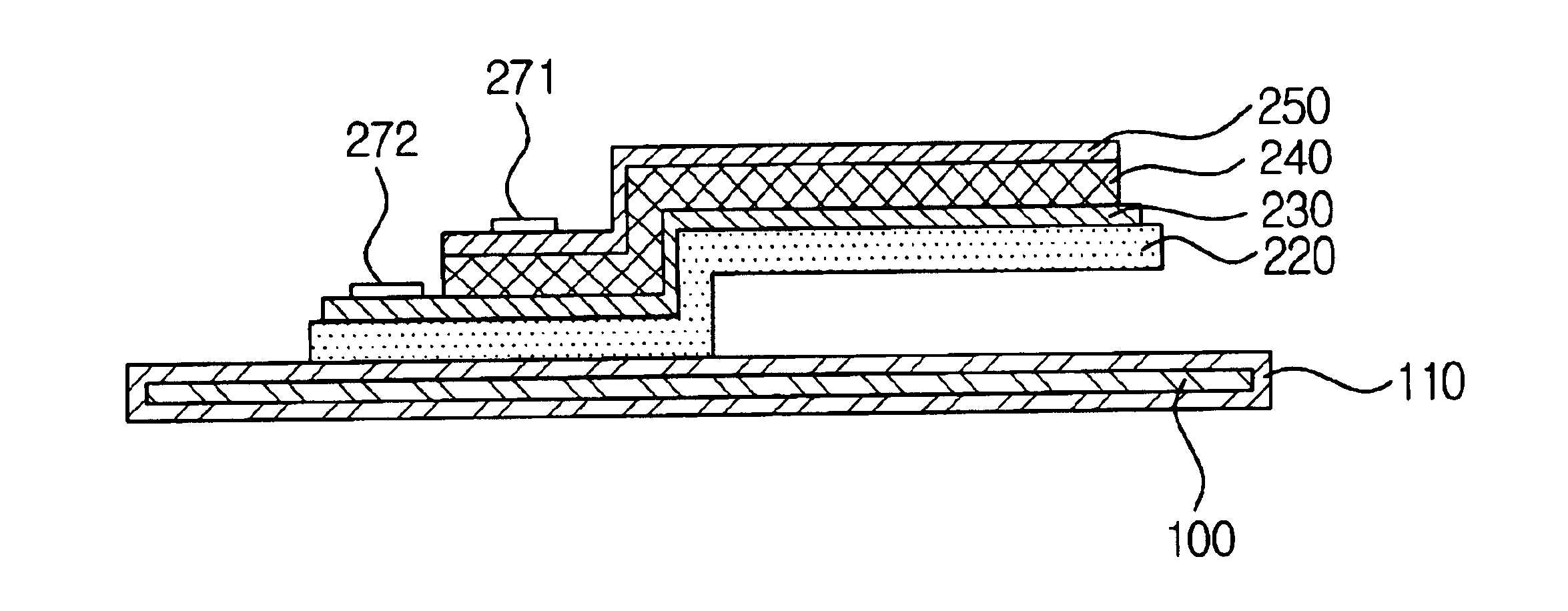
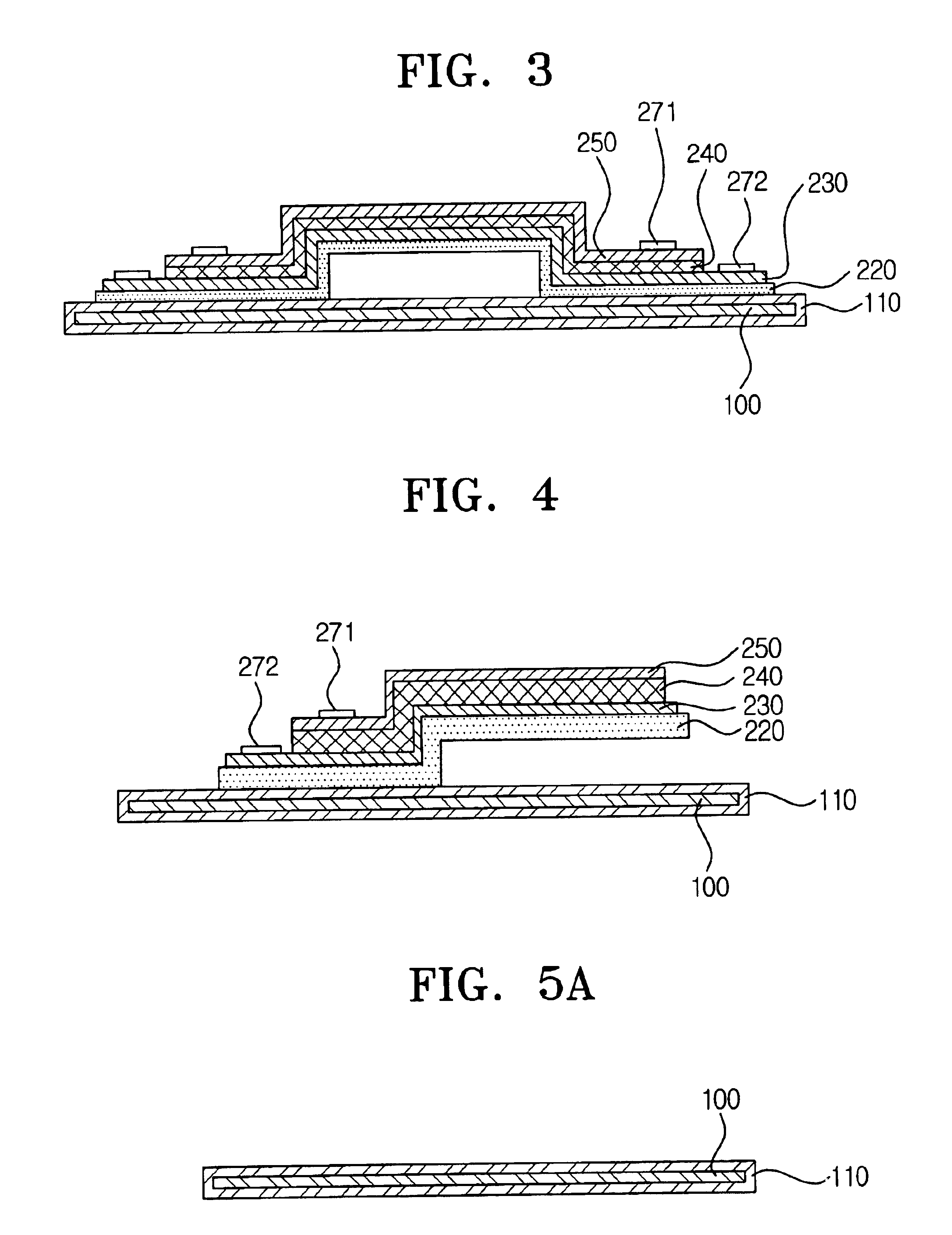
[0044]The present invention will now be described more fully hereinafter with reference to the accompanying drawings, in which preferred embodiments of the invention are shown. The invention may, however, be embodied in different forms and should not be construed as limited to the embodiments set forth herein. Rather, these embodiments are provided so that this disclosure will be thorough and complete, and will fully convey the scope of the invention to those skilled in the art. In the drawings, the thickness of layers and regions are exaggerated for clarity. It will also be understood that when a layer is referred to as being “on” another layer or substrate, it can be directly on the other layer or substrate, or intervening layers may also be present. ...


PUM


Abstract

A flexible wireless MEMS microphone includes a substrate of a flexible polymeric material, a flexible MEMS transducer structure formed on the substrate by PECVD, an antenna printed on the substrate for communicating with an outside source, a wire and interface circuit embedded in the substrate to electrically connect the flexible MEMS transducer and the antenna, a flexible battery layer electrically connected to the substrate for supplying power to the MEMS transducer, and a flexible bluetooth module layer electrically connected to the battery layer. The flexible MEMS transducer includes a flexible substrate, a membrane layer deposited on the substrate, a lower electrode layer formed on the membrane layer, an active layer formed by depositing a piezopolymer on the lower electrode layer, an upper electrode layer formed on the active layer, and a first and a second connecting pad electrically connected to the lower and upper electrode layers, respectively.

Description

BACKGROUND OF THE INVENTION[0001]1. Field of the Invention[0002]The present invention relates to a micro-electromechanical system (MEMS) structure and a method for manufacturing the same. More particularly, the present invention relates to a flexible MEMS transducer formed on a flexible substrate, a manufacturing method thereof, and a flexible MEMS wireless microphone incorporating the flexible MEMS transducer.[0003]2. Description of the Related Art[0004]In accordance with the need for very small devices, semiconductor processing technology using micromachining techniques is employed to integrate micro devices. The field of micro-electromechanical systems (MEMS) is a field of manufacturing and testing miniature sensors or actuators, which have sizes on the order of micrometers (μm), and electromechanical structures using micromachining technology applied in semiconductor processing, particularly, in integrated circuit technology.[0005]The micromachining technology employed in MEMS i...

Claims


Application Information

Patent Timeline
Patent Type & Authority Patents(United States)
IPC IPC(8): B81B3/00H04R17/02H01L41/09H01L41/193H01L41/45H04R31/00
CPCB81C1/00182H01L41/0973H01L41/094H01L41/45B81B2201/0257B81B2201/032B81B2203/0118B81B2203/0127H04R1/406H04R17/02H04R2420/07H10N30/2042H10N30/2047H10N30/098H04R31/00
Inventor NAM, YUN-WOOLEE, SUK-HAN
Owner SAMSUNG ELECTRONICS CO LTD
Why Eureka
Try Eureka