RRAM circuit with temperature compensation

a resistor memory and temperature compensation technology, applied in solid-state devices, instruments, drawing-off water installations, etc., can solve the problems of ferromagnetic ordering and metallic conductivity, information loss in dram circuits with time, and loss of information stored

Inactive Publication Date: 2005-11-22
XENOGENIC DEV LLC
View PDF5 Cites 20 Cited by
  • Summary
  • Abstract
  • Description
  • Claims
  • Application Information

AI Technical Summary

Benefits of technology

[0053]It is an objective of the present invention to provide a temperature dependent circuit to compensate for the temperature drifting of the memory resistors.
[0095]In other aspect of the invention, the present invention provides a method and a circuit comprising a temperature dependent power source to the memory resistor and a temperature dependent reference signal to the memory circuit. The addition of two temperature dependent circuits will add to the complexity of the memory circuit but will give the designer more flexibility to ensure that the memory circuit operates within the entire operating temperature range.

Problems solved by technology

In contrast to SRAM circuits, the DRAM circuits tend to lose information with time because of the inherent leakage of the capacitor charge, typically through substrate current in the memory circuits.
To replenish the charge lost by the leakage, DRAM cells must be rewritten or refreshed at frequent intervals or else the information stored will be lost.
This results in ferromagnetic ordering and metallic conductivity.
Many prior art RRAM cell reading schemes did not address the temperature dependence of the memory resistor and would be adequate if the memory resistor is temperature independent or if the temperature dependence of the memory resistor is relatively small.
The prior art constant power source (constant current source or constant voltage source) scheme to read the resistance state of a memory resistor is not adequate because the constant power source did not contain any additional information to resolve the overlapping resistance range of the memory resistor.
The problem occurs at high resistance state.
Thus at high temperature, this circuit is not able to detect high resistance state signal.
This bias scheme also works for the high temperature low resistance state of 100° C. However, it does not work at low temperature low resistance state.
Since the resistance of high resistance state at high temperatures overlaps with the resistance of low resistance state at low temperature, this circuit cannot resolve these resistance values and therefore cannot be operated in the entire temperature range.
Similar to the nMOS circuit, this pMOS circuit cannot be operated in the whole operating temperature range due to the overlapping of the resistance of the memory resistor in high resistance / high temperature and low resistance / low temperature states.
A transistor provides more access to the memory resistor at the cost of increasing circuit complexity.
Again, these circuits cannot be operated in the whole operating temperature range due to the overlapping of the resistance of the memory resistor in high resistance / high temperature and low resistance / low temperature states.

Method used


Image

  • RRAM circuit with temperature compensation
  • RRAM circuit with temperature compensation
  • RRAM circuit with temperature compensation

Examples


first embodiment

[0125]FIG. 10 shows a block diagram of the present invention. The embodiment comprises a temperature sensor block 120, providing input to a control circuit block 121. The output of the control circuit block 121 is supplied to the memory resistor array 122 before reaching a sense amplifier block 123.

[0126]The temperature sensor block 120 includes a temperature dependent element and necessary circuit to provide a temperature dependent signal to the control circuit block 121. The temperature dependent signal from the temperature sensor circuit can be a voltage or a current, and this signal varies as a function of temperature. The temperature sensor circuit can also include a signal amplifier to amplify the temperature dependent signal.

[0127]The control circuit block 121 can include variable current source. The value of the variable current source is controlled by the temperature sensor circuit. The current source then supplies to the memory resistor array 122 to provide a temperature c...

second embodiment

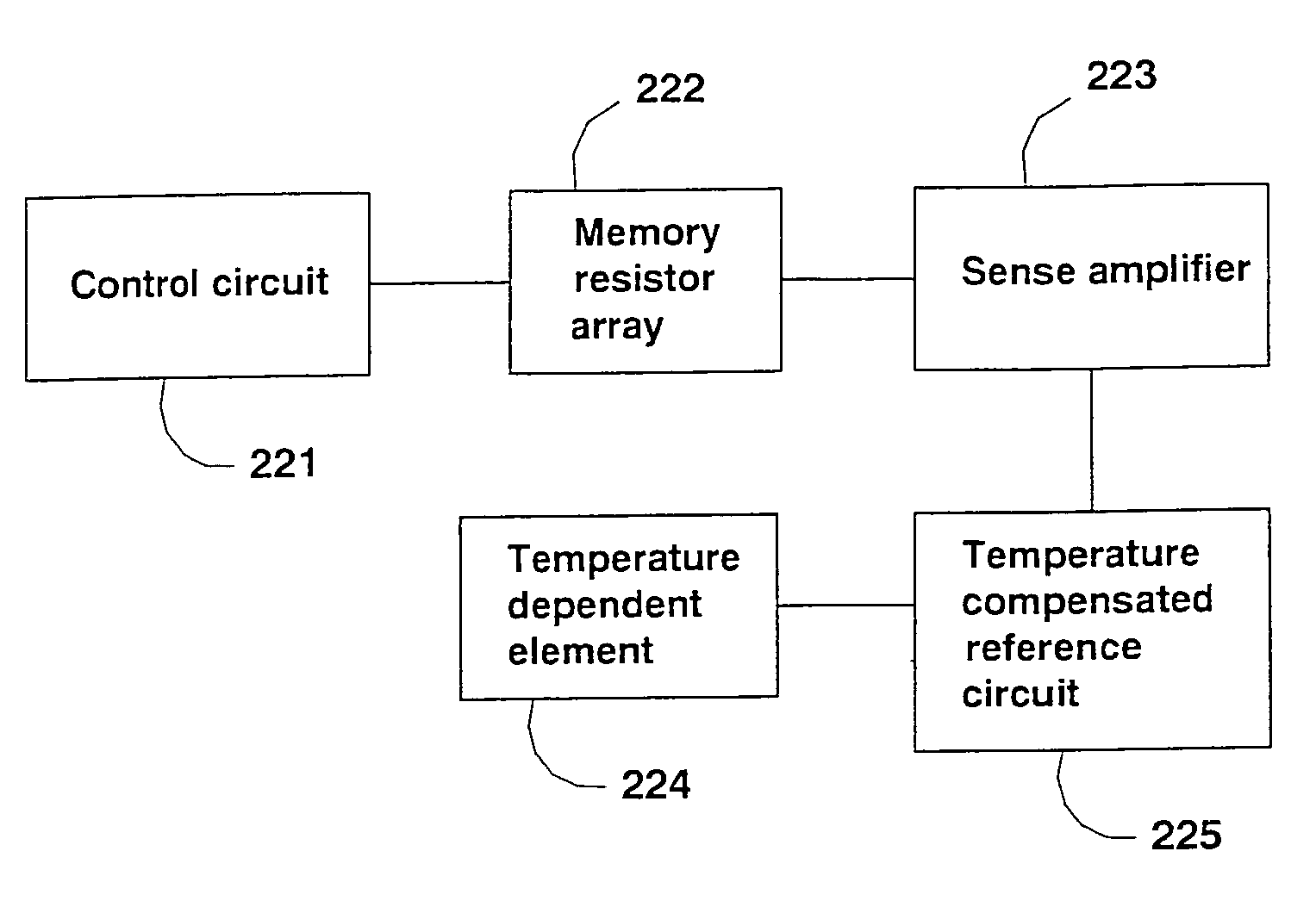
[0141]FIG. 15 shows a block diagram of the present invention. The embodiment comprises a control circuit block 221 supplying to the memory resistor array 222 before reaching a sense amplifier block 223. The sense amplifier block 223 received a reference signal from a temperature compensated reference signal circuit 225. The temperature compensated reference signal circuit 225 is taking a temperature dependent signal input from a temperature sensor 224 to control the reference signal.

[0142]The temperature sensor block 224 includes a temperature dependent element and necessary circuit to provide a temperature dependent signal to the temperature compensated reference signal circuit 225. The temperature dependent signal from the temperature sensor circuit can be a voltage or a current, and that this signal varies as a function of temperature. The temperature sensor circuit can also include a signal amplifier to amplify the temperature dependent signal.

[0143]The temperature compensated r...

third embodiment

[0147]FIG. 17 shows a block diagram of the present invention. The embodiment comprises a first temperature sensor block 320, providing input to a control circuit block 321. The output of the control circuit block 321 is supplied to the memory resistor array 322 before reaching a sense amplifier block 323. The sense amplifier block 323 received a reference signal from a temperature compensated reference signal circuit 325. The temperature compensated reference signal circuit 325 is taking a temperature dependent signal input from a second temperature sensor 324 to control the reference signal.

[0148]The first temperature sensor block 320 includes a temperature dependent element and necessary circuit to provide a temperature dependent signal to the control circuit block 321. The temperature dependent signal from the temperature sensor circuit can be a voltage or a current, and that this signal varies as a function of temperature. The temperature sensor circuit can also include a signal...


PUM


Abstract

A temperature compensated RRAM sensing circuit to improve the RRAM readability against temperature variations is disclosed. The circuit comprises a temperature dependent element to control the response of a temperature compensated circuit to generate a temperature dependent signal to compensate for the temperature variations of the resistance states of the memory resistors. The temperature dependent element can control the sensing signal supplied to the memory resistor so that the resistance states of the memory resistor are compensated against temperature variations. The temperature dependent element can control the reference signal supplied to the comparison circuit so that the output signal provided by the comparison circuit is compensated against temperature variations. The temperature dependent element is preferably made of the same material and process as the memory resistors.

Description

RELATED APPLICATIONS[0001]This application is a Divisional of a pending patent application entitled, TEMPERATURE COMPENSATED RRAM CIRCUIT, invented by Sheng Teng Hsu, Ser. No. 10 / 384,985, filed Mar. 10, 2003, now U.S. Pat. No. 6,868,025, issued on Mar. 15, 2005.BACKGROUND OF THE INVENTION[0002]The present invention relates to information storage of integrated circuit memory devices. More specifically, it relates to a temperature compensated resistor memory sensing circuit.[0003]Integrated circuit (IC) memory devices have replaced magnetic-core memory devices due to their lower fabrication cost and higher performance. An IC memory circuit includes a repeated array of memory cells which store one state of a two state information (0 or 1), or multi-state information (for example, 00, 01, 10, or 11 of 4 states), together with support circuitries such as a row decoder, a column decoder, a write circuit to write to the memory cell array, a control circuitry to select the correct memory ce...

Claims


Application Information

Patent Timeline
Patent Type & Authority Patents(United States)
IPC IPC(8): G11C16/02G11C13/00G11C11/56G11C7/00G11C7/06G11C7/14G11C13/02G11C7/04H01L27/10
CPCG11C7/04G11C7/062G11C7/067G11C7/14G11C11/5678G11C11/5685G11C13/0007G11C13/004G11C2213/79G11C2013/0054G11C2213/31G11C2213/72G11C13/0004E03B9/10G01F15/10
Inventor HSU, SHENG TENG
Owner XENOGENIC DEV LLC
Why Eureka
Try Eureka