Wavefront aberration measuring instrument, wavefront aberration measuring method, exposure apparatus, and method for manufacturing micro device

a technology of exposure apparatus and measurement instrument, which is applied in the direction of instruments, optical radiation measurement, printers, etc., can solve the problems of insufficient assurance of accuracy of measurement of aberration and long measurement time, so as to improve exposure accuracy, accurately measure wavefront aberration of projection optical system, and high manufacturing accuracy

Inactive Publication Date: 2005-12-13
NIKON CORP
View PDF35 Cites 38 Cited by
  • Summary
  • Abstract
  • Description
  • Claims
  • Application Information

AI Technical Summary

Benefits of technology

[0012]The present invention has been achieved paying attention to such problems existing in the prior art. It is an object of the present invention to provide a wavefront aberration measuring instrument and a wavefront aberration measuring method which can accurately measure a wavefront aberration of a target optical system such as a projection optical system. Moreover, it is another object of the present invention to provide an exposure apparatus which can accurately measure a wavefront aberration of a projection optical system and improve exposure accuracy, and a method for manufacturing a micro device by which a micro device can be highly accurately manufactured.

Problems solved by technology

However, the prior art method has a problem that the accuracy of measuring the aberration can not be sufficiently assured due to a manufacturing error of a pattern of the mask for aberration measurement, irregularities of application of the photoresist, a processing error of development unevenness or the like.
Further, in observation using the SEM, a predetermined pretreatment for the substrate, for example, a development process or the like of the substrate is required, and it takes a long time for measuring the aberration.

Method used


Image

  • Wavefront aberration measuring instrument, wavefront aberration measuring method, exposure apparatus, and method for manufacturing micro device
  • Wavefront aberration measuring instrument, wavefront aberration measuring method, exposure apparatus, and method for manufacturing micro device
  • Wavefront aberration measuring instrument, wavefront aberration measuring method, exposure apparatus, and method for manufacturing micro device

Examples


Embodiment Construction

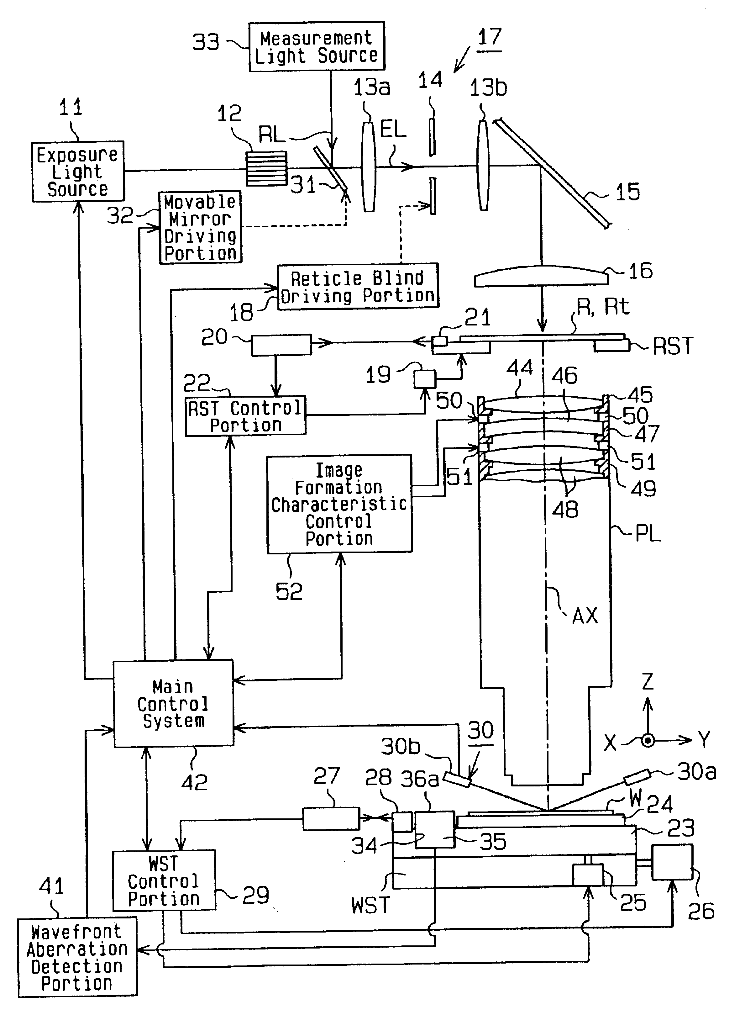
[0027]A first embodiment according to the present invention in an exposure apparatus which is of a scanning exposure type for manufacturing a semiconductor element will now be described below with reference to FIGS. 1 to 4.

[0028]A schematic structure of the exposure apparatus will be first explained.

[0029]As shown in FIG. 1, an exposure light source 11 emits pulse exposure light EL, such as KrF excimer laser beam, ArF excimer laser beam, or F2 laser beam. The exposure light EL enters, for example, a fly-eye lens 12 consisting of many lens elements as an optical integrator, and many secondary light source images corresponding to the respective lens elements are formed on an emission surface of the fly-eye lens 12. It is to be noted that a rod lens may be adopted as the optical integrator. The exposure light EL emitted from the fly-eye lens 12 enters a reticle R as a mask mounted on a reticle stage RST through relay lenses 13a and 13b, a reticle blind 14, a mirror 15 and a condenser l...


PUM

PropertyMeasurementUnit
oscillation wavelengthaaaaaaaaaa

Abstract

Before measuring a wavefront aberration of a projection optical system, an image formation position of an image of a pattern of a test reticle which is formed on a predetermined surface is detected by an AF sensor. Based on a result of this detection, the position of an incident surface of a wavefront aberration measurement unit is adjusted, and a position of an image of the pattern with respect to the incident surface is adjusted. After this adjustment, the image of the pattern formed through the projection optical system is detected by the wavefront aberration measurement unit, and a wavefront aberration detection section is used to obtain wavefront aberration information of the projection optical system based on a result of this detection.

Description

RELATED APPLICATION[0001]This application is a continuation of PCT application number PCT / JP01 / 11274 filed on Dec. 21, 2001.BACKGROUND OF THE INVENTION[0002]The present invention relates to a wavefront aberration measuring instrument for measuring a wavefront aberration of a target optical system such as a projection optical system in an exposure apparatus used in a photolithography step in a manufacturing process of a micro device such as a semiconductor element, a liquid crystal display element device, an image pickup element or a thin-film magnetic head, a wavefront aberration measuring method, an exposure apparatus having the wavefront aberration measuring instrument, and a method for manufacturing the above-described micro device.[0003]There has been conventionally known an exposure apparatus which illuminates an image of a pattern formed on a mask, such as a reticle or a photo mask, with exposure light and transfers the image of the pattern onto a substrate such as a wafer or ...

Claims


Application Information

Patent Timeline
Patent Type & Authority Patents(United States)
IPC IPC(8): G01M11/02G03F7/20G03F9/00
CPCG01M11/0264G01M11/0271G03F7/706G03F9/7026
Inventor MIZUNO, YASUSHI
Owner NIKON CORP
Why Eureka
Try Eureka