
Method of manufacturing a semiconductor device

a manufacturing method and semiconductor technology, applied in semiconductor devices, instruments, optics, etc., can solve the problems of increasing the frequency of contact failure, pixel pitch reduction, and limited method of mounting a driver i

Inactive Publication Date: 2005-12-27
SEMICON ENERGY LAB CO LTD
View PDF77 Cites 15 Cited by
  • Summary
  • Abstract
  • Description
  • Claims
  • Application Information

AI Technical Summary

Benefits of technology

[0011]The present invention has been made to solve those problems, and an object of the present invention is therefore to provide a technique of obtaining TFT structures optimal for driving conditions of a pixel portion and driving circuits using a small number of photo masks.

Problems solved by technology

However, mounting a driver IC is considered as a limited method because the pixel pitch is reduced as the pixel density is increased.
An increase in number of connection terminals leads to increased occurrence of contact failure.
It also leads to an increase in area of the border surrounding the pixel portion (called a picture frame region), which hinders reduction in size of a semiconductor device that employs this display and spoils the external design of the semiconductor device.
If optimization of TFT structures to suit what are demanded for the pixel portion and the driving circuits is dealt with by simply increasing the number of photo masks, the manufacture process becomes complicated and the number of steps is increased inevitably.

Method used


Image

  • Method of manufacturing a semiconductor device
  • Method of manufacturing a semiconductor device
  • Method of manufacturing a semiconductor device

Examples


embodiment mode 1

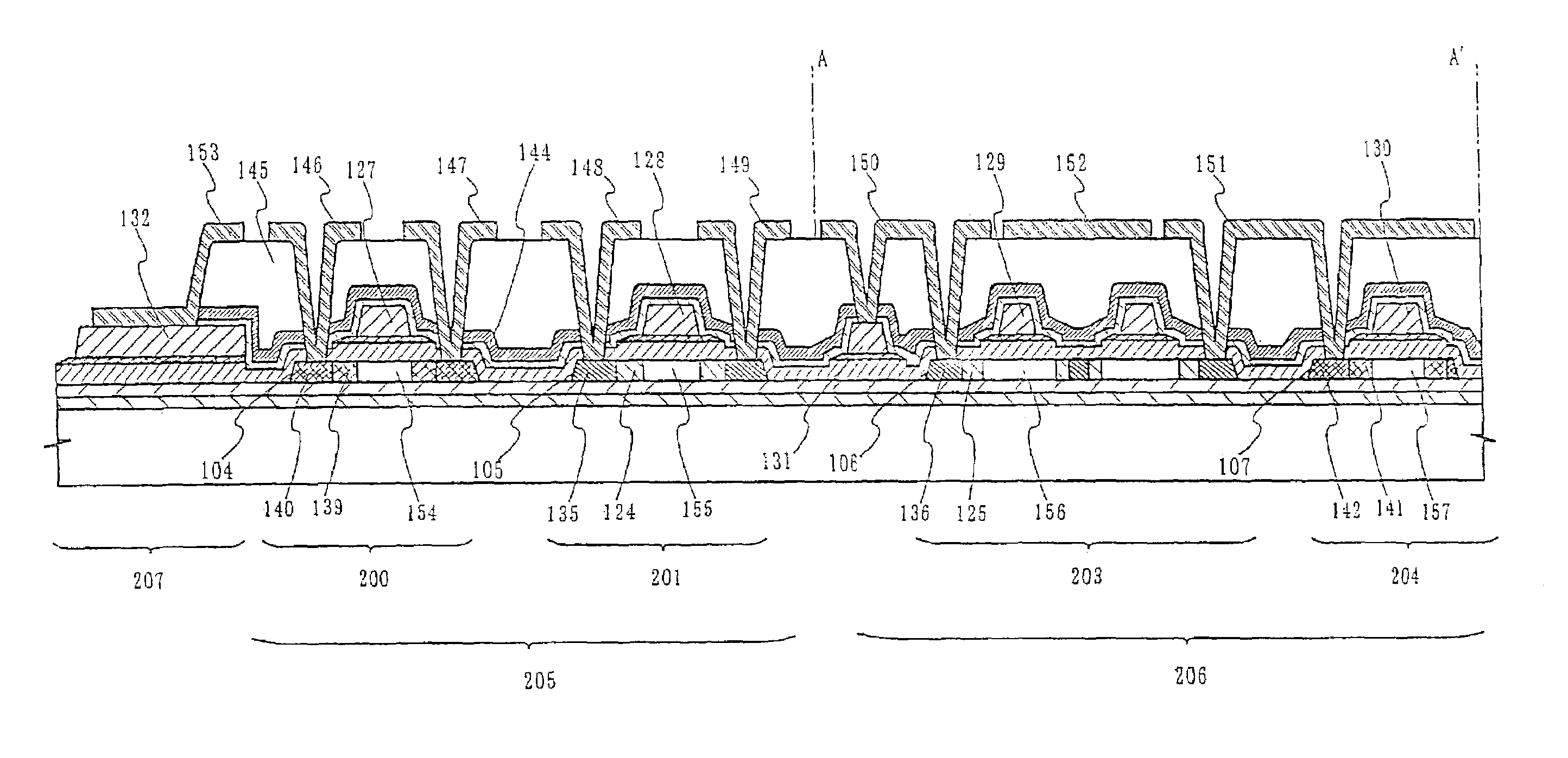
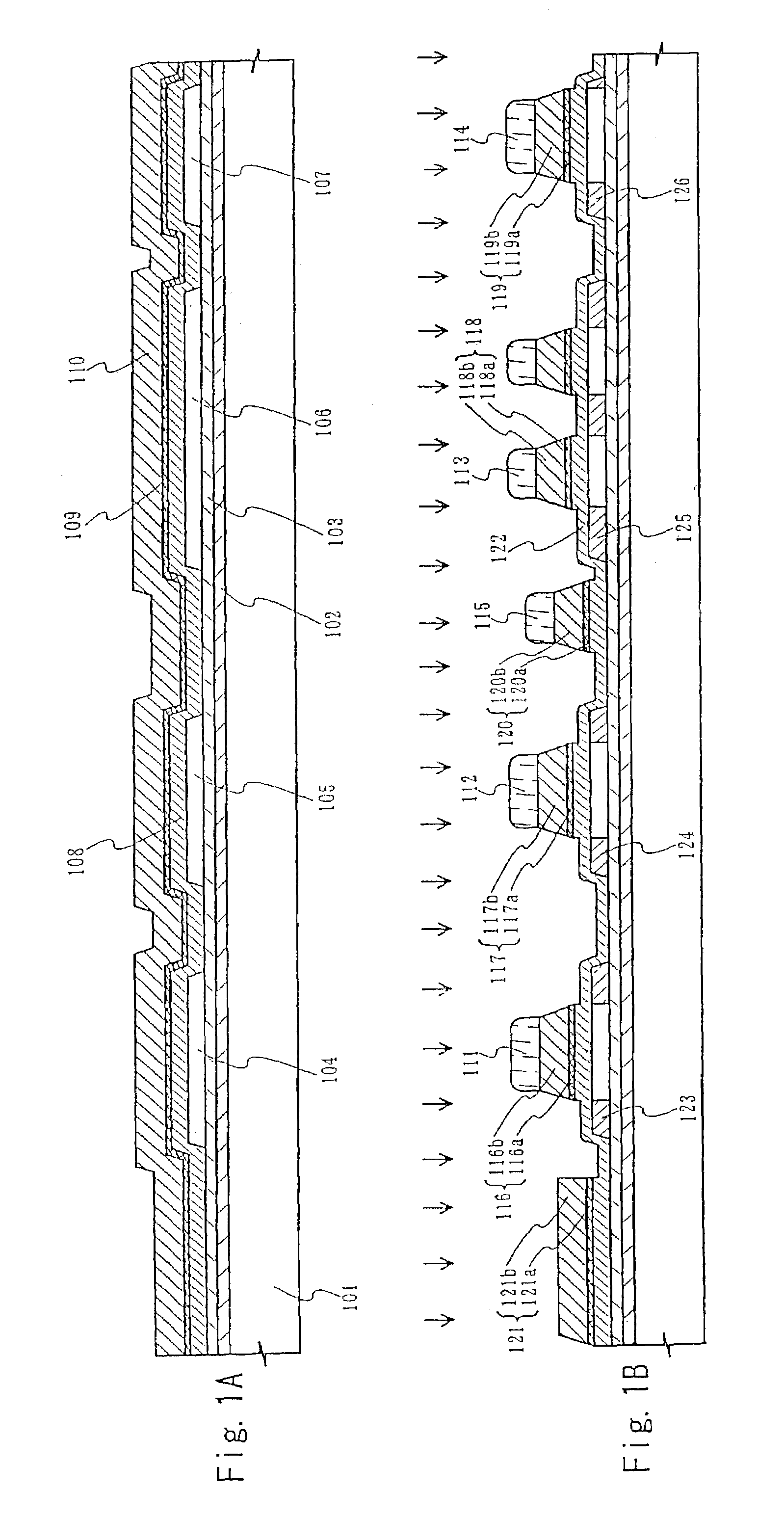
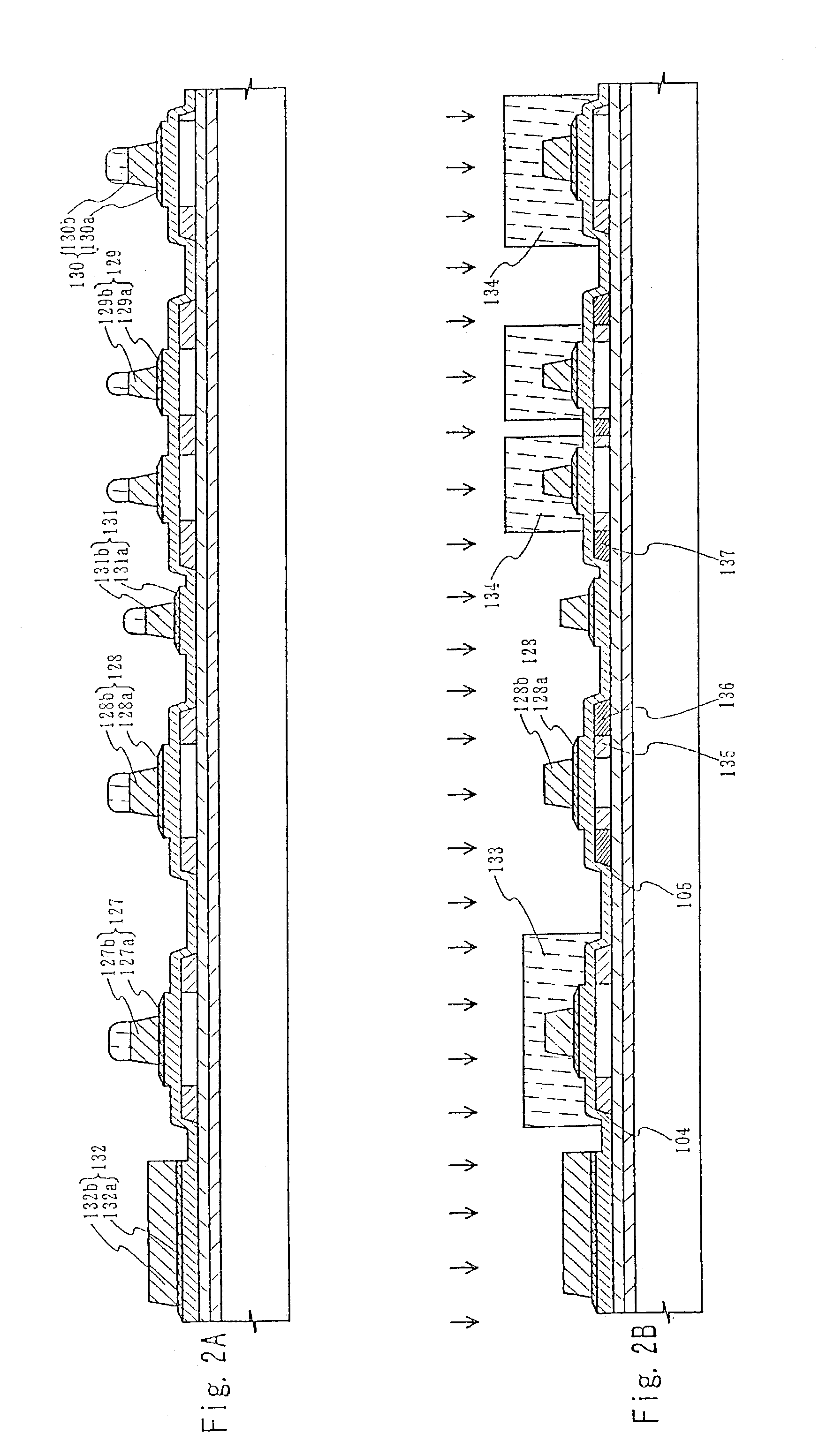
[0055]An embodiment mode of the present invention will be described with reference to FIGS. 1A to 6. Here, a detailed description is given on a method of simultaneously forming on the same substrate a TFT for a pixel portion and TFTs (an n-channel TFT and a p-channel TFT) for driving circuits that are placed near the pixel portion.

[0056]In FIG. 1A, a substrate 101 is a glass substrate, a quartz substrate, or a ceramic substrate. A silicon substrate, metal substrate or stainless steel substrate, with an insulating film formed on its surface may be used instead. A plastic substrate may also be used if it has a heat resistance that can withstand the process temperature of this embodiment mode.

[0057]First insulating films 102 and 103 are formed on the substrate 101. The first insulating films shown here have a two-layer structure but they may of course have a single layer structure. Semiconductor films 104 to 107 are semiconductors having a crystal structure. The semiconductor films are...

embodiment mode 2

[0080]Another embodiment mode of the present invention will be described with reference to FIGS. 7A to 10. Here, a detailed description is given on a method of simultaneously forming on the same substrate a TFT for a pixel portion and TFTs (an n-channel TFT and a p-channel TFT) for driving circuits that are placed in the periphery of the pixel portion.

[0081]The description on the substrate, the insulating films, the semiconductor films, and the conductive films in Embodiment Mode 1 applies to a substrate 301, first insulating films 302 and 303, semiconductor films 304 to 307, a second insulating film 308, a first conductive film 309, and a second conductive film 310 in FIG. 7A.

[0082]Masks 311 and 312 are formed in FIG. 7B. The mask 311 covers the driving circuit portion whereas the mask 312 covers the pixel portion. With the masks covering the pixel and driving circuit portions, the first conductive film and the second conductive film are etched in first etching treatment to form a ...

embodiment 1

[0095]An embodiment of the present invention will be described below with reference to FIG. 1A to FIG. 6. Here, a detailed description is given on a method of simultaneously forming on the same substrate a TFT for a pixel portion and TFTs (an n-channel TFT and a p-channel TFT) for driving circuits that are placed in the periphery of the pixel portion.

[0096]In FIG. 1A, alumino borosilicate glass is used for a substrate 101. A first insulating film is formed on the substrate 101. The first insulating film in this embodiment is a laminate of a first silicon oxynitride film 102 with a thickness of 50 nm and a second silicon oxynitride film 103 with a thickness of 100 nm. The film 102 is formed using as reaction gas SiH4, NH3, and N2O. The film 103 is formed using as reaction gas SiH4 and N2O.

[0097]Semiconductor films 104 to 107 are semiconductors having a crystal structure. The semiconductor films are obtained by forming an amorphous semiconductor film on the first insulating film and c...


PUM

PropertyMeasurementUnit
angleaaaaaaaaaa
thicknessaaaaaaaaaa
angleaaaaaaaaaa

Abstract

TFT structures optimal for driving conditions of a pixel portion and driving circuits are obtained using a small number of photo masks. First through third semiconductor films are formed on a first insulating film. First shape first, second, and third electrodes are formed on the first through third semiconductor films. The first shape first, second, third electrodes are used as masks in first doping treatment to form first concentration impurity regions of one conductivity type in the first through third semiconductor films. Second shape first, second, and third electrodes are formed from the first shape first, second, and third electrodes. A second concentration impurity region of the one conductivity type which overlaps the second shape second electrode is formed in the second semiconductor film in second doping treatment. Also formed in the second doping treatment are third concentration impurity regions of the one conductivity type which are placed in the first and second semiconductor films. Fourth and Fifth concentration impurity regions having the other conductivity type that is opposite to the one conductivity type are formed in the third semiconductor film in third doping treatment.

Description

BACKGROUND OF THE INVENTION[0001]This application is a div of Ser. No. 10 / 078,414 U.S. Pat. No. 6,599,785.[0002]1. Field of the Invention[0003]The present invention relates to a semiconductor device with a thin film transistor (hereinafter referred to as TFT) formed of a semiconductor film that has a crystal structure and is formed on a substrate, and to a method of manufacturing the semiconductor device.[0004]2. Description of the Related Arts[0005]A display for displaying text and images is indispensable means for people to digest information with various semiconductor devices that have semiconductor elements, such as television sets, personal computers; and cellular phones. CRTs have long, been in the market to acquire the position of representative display. On the other hand, liquid, crystal displays and other flat displays (flat panel displays), are lately increasing their shares exponentially, for electronic devices are desired to reduce weight and size.[0006]One mode of flat ...

Claims


Application Information

Patent Timeline
Patent Type & Authority Patents(United States)
IPC IPC(8): H01L29/786G02F1/1362H01L21/77H01L21/84H01L27/12H01L29/423
CPCH01L27/1214H01L29/42384G02F1/13454H01L27/124H01L27/127H01L27/12H01L29/4908
Inventor HAMADA, TAKASHIARAI, YASUYUKI
Owner SEMICON ENERGY LAB CO LTD
Learn More