Program for controlling laser apparatus and recording medium for recording program for controlling laser apparatus and capable of being read out by computer

a laser and recording medium technology, applied in the direction of programme control, total factory control, instruments, etc., can solve the problems of reducing the current transportation characteristics of carriers, reducing and reducing so as to improve the treatment rate of substrates and shorten the time required for irradiation

Inactive Publication Date: 2008-01-10
SEMICON ENERGY LAB CO LTD
View PDF99 Cites 3 Cited by
  • Summary
  • Abstract
  • Description
  • Claims
  • Application Information

AI Technical Summary

Benefits of technology

[0017] The present invention shortens a substrate treatment time by using a computer and thereby obtaining an optimum control method of a laser treatment drive in accordance with proper laser irradiation information obtained from a combination of CAD masks for a silicon island, contact, and wiring metal and controlling a laser treatment system in accordance with the obtained laser-treatment-drive control method.
[0031] means for obtaining an optimum driving condition of a laser system for minimizing the laser treatment time required for the above one substrate by considering the speed of each drive of a laser system and the time required for changing drives of the laser system in accordance with the positional information on the silicon island, formal information on the silicon island, and directional information on the source, channel, and drain of the silicon island stored in the database; and
[0036] means for obtaining an optimum driving condition of a laser system for minimizing the laser treatment time required for the above one substrate by considering the speed of each drive of a laser system, the time required for changing drives of the laser system, and the time required for the computer to generate a driving command for each drive and thereafter for each drive to start actual driving in accordance with the positional information on the silicon island, formal information on the silicon island, and directional information on the source, channel, and drain of the silicon island stored in the database; and
[0042] means for minimizing the laser processing time required for the above one substrate and obtaining an optimum driving condition of a laser system by considering the speed of each drive of a laser system, the time required for changing drives of the laser system, and the time required for the computer to generate a driving command for each drive and thereafter for each drive to start actual driving; and
[0048] The above configuration makes it possible to shorten the time required for irradiation with a laser beam and improve the treatment rate of a substrate.

Problems solved by technology

It is known that this reduces current transportation characteristics of carriers due to an influence of a potential barrier in a recombination center or a trapping center of the carriers or in the grain boundary, which is caused by a crystal defect or the like, and causes an OFF current to increase in the TFT.
Thus, it is impossible to designate the position and the size of the crystal grain to form the TFT.
Also, since a range of the energy intensity region is extremely narrow, from a viewpoint of position control of the crystal grain, it is impossible to control positions where the crystal grains having a large grain size are obtained.
However, it involves the following problems.
First, as a first problem, there can be cited poor substrate processing efficiency (throughput).
Needless to say, however, the crystal peculiar to the SLS method cannot be manufactured under the above condition.
The fact that a large amount of processing time per substrate is required does not lead to only a problem in terms of time or cost.
Further, this may finally cause a variation in characteristics of a transistor in the substrate surface.
As a second problem, there can be cited the optical system that tends to be complicated in the conventional SLS method.
It is difficult to manufacture a slit-like mask resistant to such a high laser energy density.
As described above, the conventional SLS method involves the complicated optical system and a factor making device maintenance difficult to perform.
Thus, processing efficiency is poor and it is an important object to improve the processing speed of the substrate.

Method used


Image

  • Program for controlling laser apparatus and recording medium for recording program for controlling laser apparatus and capable of being read out by computer
  • Program for controlling laser apparatus and recording medium for recording program for controlling laser apparatus and capable of being read out by computer
  • Program for controlling laser apparatus and recording medium for recording program for controlling laser apparatus and capable of being read out by computer

Examples


example 1

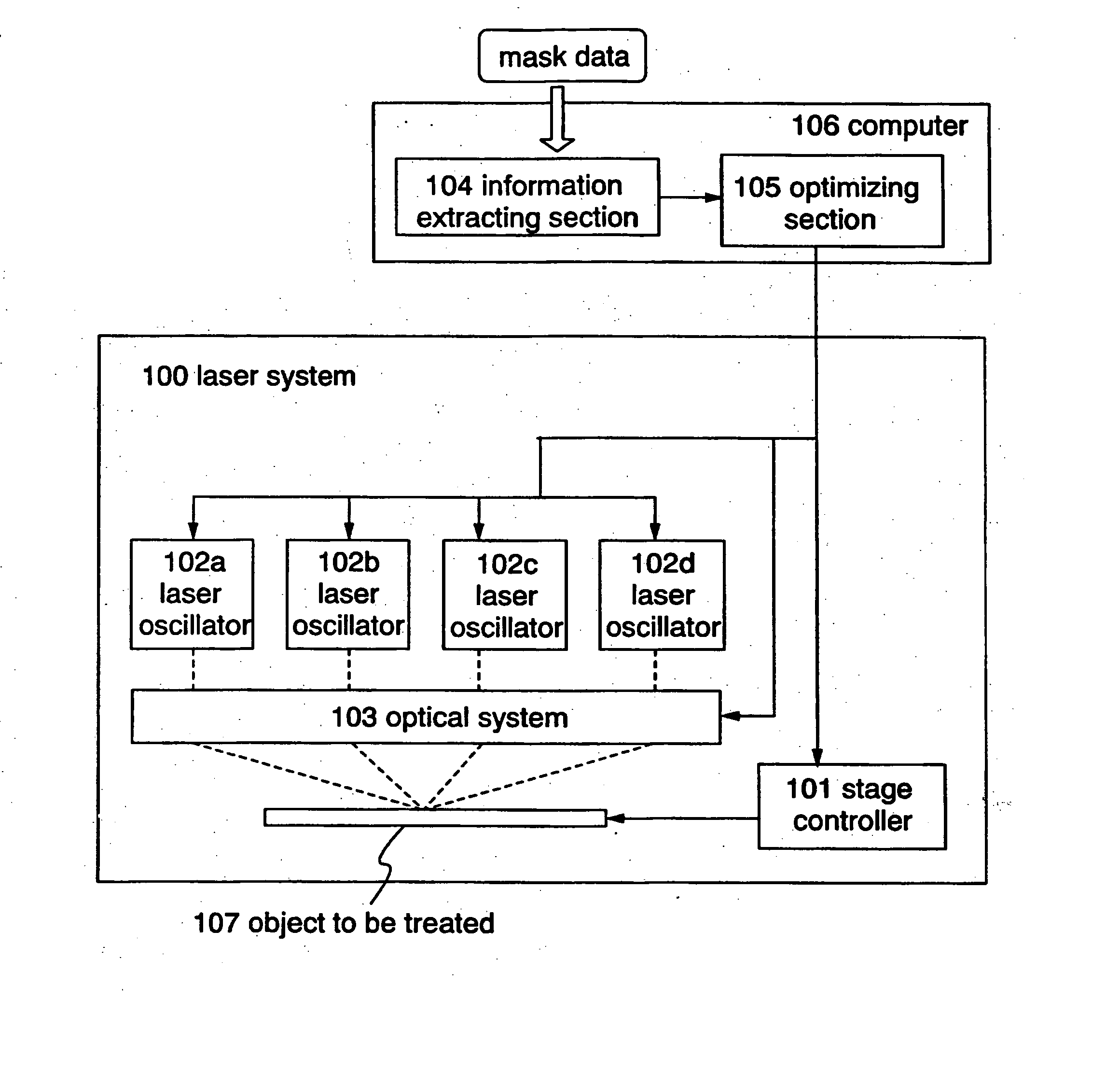
[0102] For this example, the information extracting section 104 of the present invention in FIG. 1 is described.

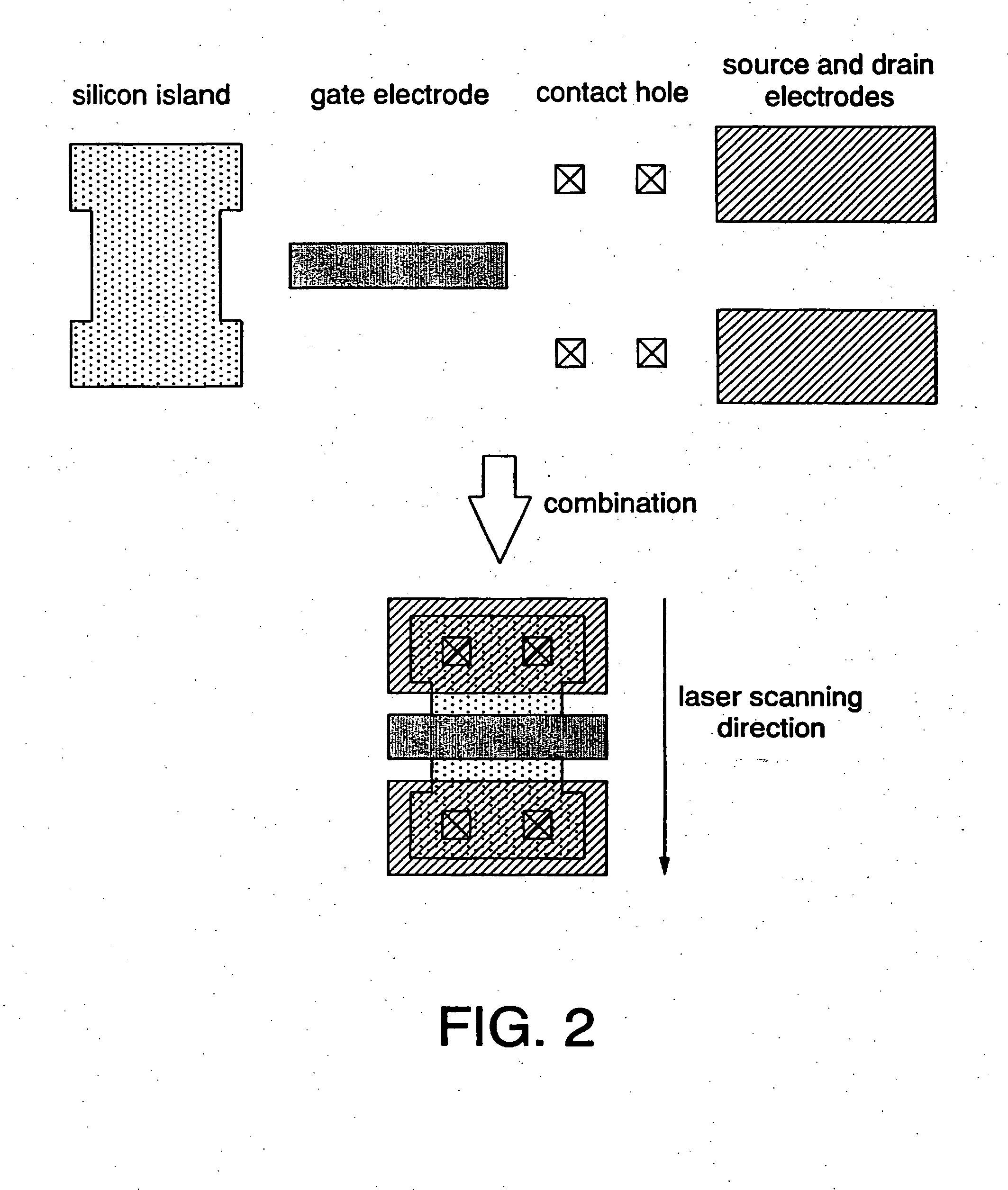
[0103]FIG. 2 shows CAD mask drawings for a silicon island, contact, and wiring metal and a combined mask drawing. It is originally possible to obtain the information on a position and shape to be crystallized by a laser in accordance with only the information on a silicon mask. However, the present system makes it possible to obtain the directional information on the source→channel→drain (or drain→channel→source) of a silicon island by also processing CAD mask drawings of a contact and wiring metal in addition to a CAD mask for a silicon island from the viewpoint of also placing great importance on the difference between transistor characteristics depending on a laser scanning direction.

[0104] In the case of a mask drawing, it is possible to obtain the directional information on a silicon island in accordance with the mutual arrangement of CAD mask drawings of the silico...

example 2

[0107] For this example, a method for obtaining a high-working-efficiency condition in accordance with the information obtained by an optimizing section from an information extracting section is described.

[0108] It is an object of an optimizing section to optimize a control method by considering the speed of a drive, the time required to change a drive to a different drive, and the time required from generation of a driving command up to actual driving when capturing the position, shape, and size of a silicon island extracted from a combination of CAD masks of the silicon island, a contact, and a wiring metal and the directional information on the source, channel, and drain of the silicon island and driving a laser, mirror, slit, and stage. Optimizing algorithms such as a linear programming method, branch and bound method, neuron circuit network, and annealing method are present in a specific optimizing method. An optimizing algorithm slightly depends on a device to be driven. Howe...

example 3

[0113] In the case of operations by an optimizing section, it is important to sufficiently consider the speed of a drive, the time required to change a drive to a different drive, and the time required from generation of a driving command up to actual driving when driving a laser, mirror, slit, and stage. When constituting software, it is necessary to sufficiently comprehend the scale for these times. Therefore, the processing time by an actual driving system is described below.

[0114] A stage moving in x and y directions indispensable for scanning for deciding a position to be irradiated by a laser is one of important drives. The moving speed of the stage ranges between several and thousands of mm / sec. In fact, however, an acceleration period is present from the start of driving the stage up to reaching a certain speed and a deceleration period is present up to end of driving the stage. The acceleration-deceleration time of the acceleration period and deceleration period is decided...


PUM


Abstract

The object of the present invention is to solve problems of treatment time when using an SLS method or continuous-oscillation laser. An indispensable portion is scanned with a laser beam in order to crystallize a semiconductor film by driving a laser and so on in accordance with the positions of islands instead of scanning and irradiating the whole semiconductor film. The present invention makes it possible to omit the time for irradiating a portion to be removed through patterning after crystallizing the semiconductor film with a laser beam and greatly shorten the treatment time for one substrate.

Description

BACKGROUND OF THE INVENTION [0001] 1. Field of the Invention [0002] The present invention relates to the software for controlling a laser treatment system for crystallizing a semiconductor substrate or semiconductor film by a laser beam or activating the substrate or film after ion-implanting it by a computer or a computer-readable recording medium. [0003] 2. Description of the Related Art [0004] As an example of a method of forming the active layer of the thin film transistor (hereinafter, referred to as TFT), there has been developed a technique of forming an amorphous semiconductor film on a substrate having an insulating surface to crystallize the film through a laser annealing method, a thermal annealing method, or the like. [0005] The laser annealing method is known as crystallization technique, which makes it possible to apply high energy only to the amorphous semiconductor film to crystallize the film without significantly increasing a temperature of a glass substrate. In pa...

Claims


Application Information

Patent Timeline
Patent Type & Authority Applications(United States)
IPC IPC(8): H01L21/76H01L21/324G05B19/4097
CPCG05B2219/45027G05B19/4097Y02P90/02H01L21/324
Inventor MIYANAGA, AKIHARUMUKAO, KYOUICHI
Owner SEMICON ENERGY LAB CO LTD
Why Eureka
Try Eureka