Semiconductor device and manufacturing method thereof

a semiconductor and semiconductor technology, applied in the direction of semiconductor devices, electrical devices, transistors, etc., can solve the problems of increasing the number of photomasks, increasing the number of photomasks, and so as to achieve low off current and increase production costs. , the effect of increasing the number of manufacturing process steps

Inactive Publication Date: 2007-11-20
SEMICON ENERGY LAB CO LTD
View PDF40 Cites 3 Cited by
  • Summary
  • Abstract
  • Description
  • Claims
  • Application Information

AI Technical Summary

Benefits of technology

[0010]With the aim of solving these problems, an object of the present invention is to provide a TFT having a low off current at a small pixel size (small TFT size), and to provide a technique for achieving optimal TFT structures for the driving conditions of a pixel portion and driver circuits by using a small number of photomasks.
[0011]Further, an object of the present invention is to provide a technique of making different TFTs, having a low off current and having TFT structures optimal for the driving conditions of a pixel portion and driver circuits, without increasing the number of manufacturing processes or the production costs.
[0017]The semiconductor device disclosed by the present invention has a region which contains a second concentration impurity element and which overlaps with a gate electrode through a gate insulating film, and an impurity region which contains a first concentration impurity element and which does not overlap with the gate electrode. The region containing the second concentration impurity element has an impurity region (Loff region) which contains the first concentration impurity element and which does not overlap with the gate electrode. By possessing this Loff region, the width of the energy barrier of PN junctions formed within the semiconductor layer becomes broader, the electric field strength added to the PN junction portions becomes weaker, and the off current can be reduced. Further, by having the impurity region (Lov region) which contains the second concentration of the impurity and which overlaps with the gate electrode through the gate insulating film, this becomes a structure in which on current degradation is prevented. A semiconductor device having high reliability can therefore be obtained.
[0028]TFTs meeting the demands of different circuits can thus be formed separately on the same substrate without increasing the number of manufacturing process steps and without increasing production costs. Thus, a semiconductor device having a low off current and high reliability can be manufactured.

Problems solved by technology

There has been a problem with TFTs containing active layers having a crystalline structure, which are recently used more and more due to their high field effect mobility, in that the off current becomes large.
There are limitations on making the wiring width narrower for increase of the aperture ratio, considering problems such as a rise of the wiring resistance.
Therefore, if the TFT structure is optimized according to the requirements of the pixel portion or each driver circuit, then the number of photomasks simply increases, the manufacturing processes become complex, and the number of process steps inevitably increases.
Further, TFTs having a sufficiently low off current cannot be manufactured even if small TFTs are manufactured in order to increase the aperture ratio in the pixel portion, and the reliability drops.
It is not easy to manufacture the desired display device (semiconductor device).

Method used


Image

  • Semiconductor device and manufacturing method thereof
  • Semiconductor device and manufacturing method thereof
  • Semiconductor device and manufacturing method thereof

Examples


embodiment mode 1

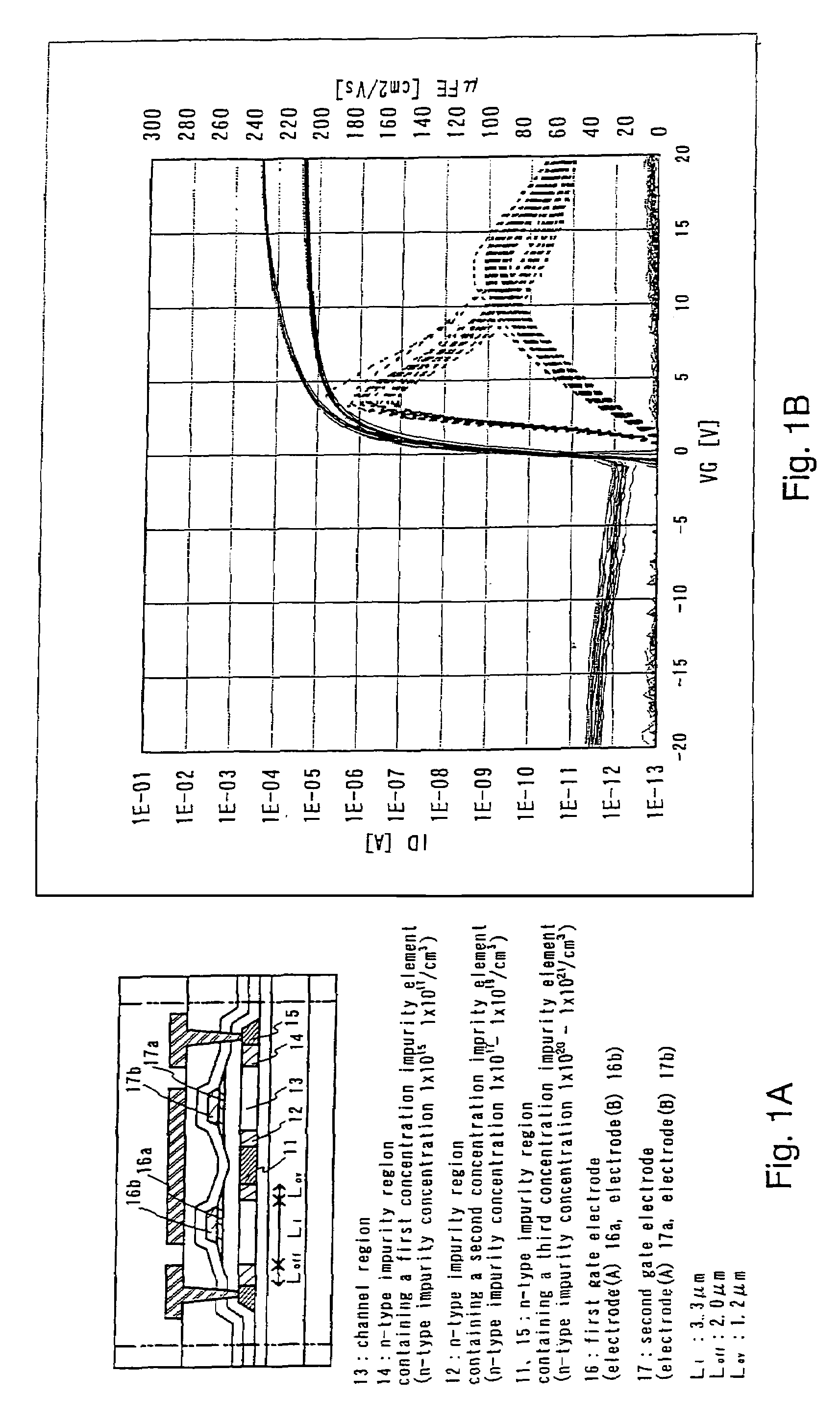
[0046]The structure of a TFT of the present invention is shown in FIG. 1A, and the results of measuring the electrical characteristics of the TFT of the present invention are shown in FIG. 1B.

[0047]The TFT has a semiconductor layer on an insulating surface, a gate insulating film on the semiconductor layer, and a gate electrode on the gate insulating film. The semiconductor layer contains a channel forming region 13, an n-type impurity region 14 containing a first concentration impurity element which imparts n-type conductivity (hereafter referred to as n-type impurity element), an n-type impurity region 12 containing a second concentration of the n-type impurity element, and n-type impurity regions 11 and 15 containing a third concentration of the n-type impurity element. The gate electrode has a first gate electrode 16 and a second gate electrode 17. The first gate electrode and the second gate electrode are composed of electrodes (A) 16a and 17a, and electrodes (B) 16b and 17b, r...

embodiment mode 2

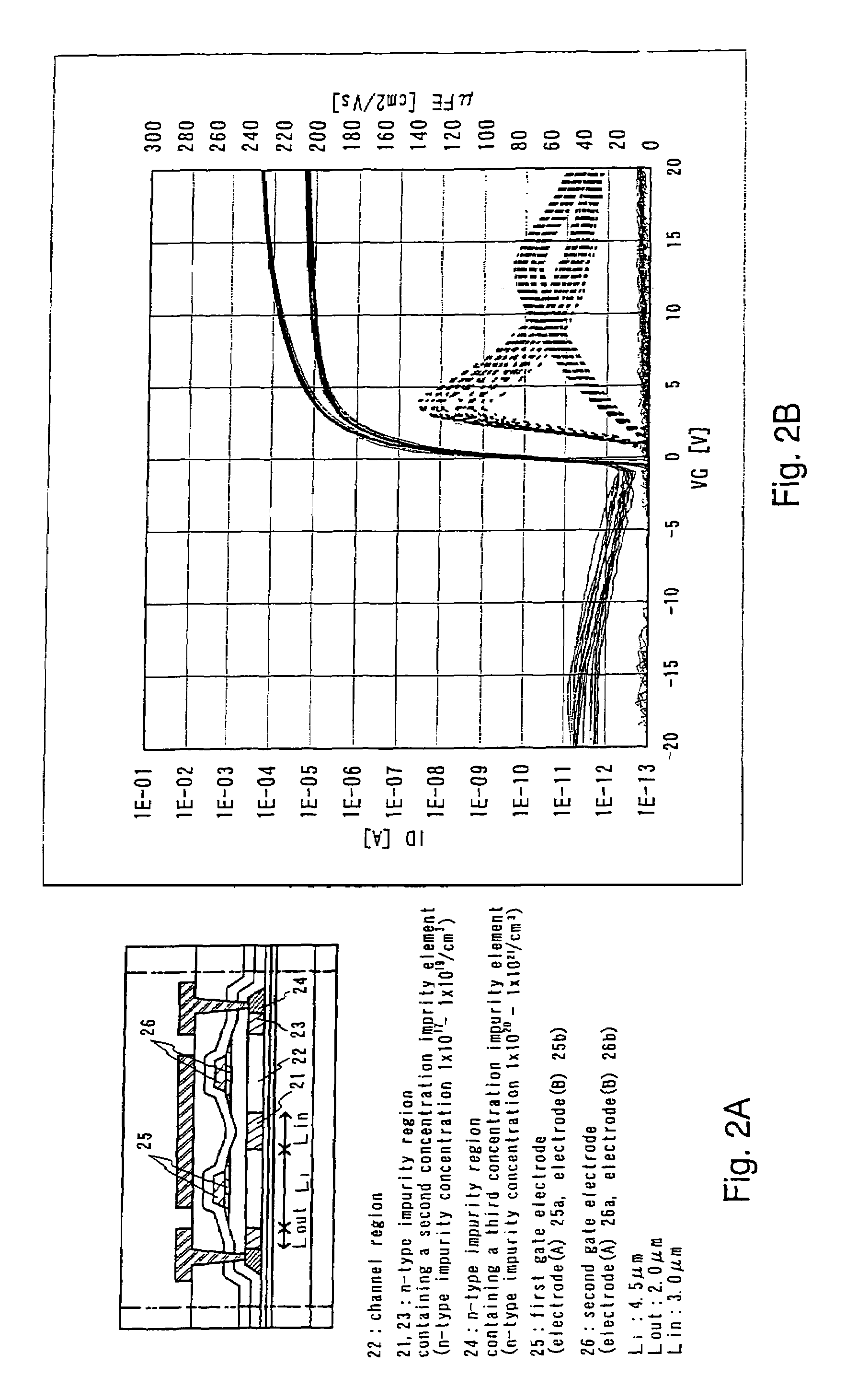
[0055]The electrical characteristics of TFTs manufactured by setting the size between a plurality of gate electrodes (two gate electrodes in Embodiment Mode 2) equal to 2 μm, for multi-gate TFTs having the TFT structure disclosed by the present invention (refer to FIG. 1A) and for those having the TFT structure already disclosed by a conventional technique (refer to FIG. 2A), are compared in Embodiment Mode 2.

[0056]Measurements were performed with the gate voltage VG varied from −20 to 20 V, and the source voltage VS=0 V. The results of measuring the current (on current) at the following two points: (1) the drain voltage VD=1 V and VG=10 V; and (2) the drain voltage VD=14 V and VG=10 V, and the results of measuring the current (off current) at the following two points: (3) VD=1 V and VG=−17.5 V; and (4) VD=14 V and VG=−4.5 V, are shown in FIGS. 14A to 14D, respectively.

[0057]The on current at the measurement points (1) and (2) is higher with the structure of the present invention co...

embodiments

Embodiment 1

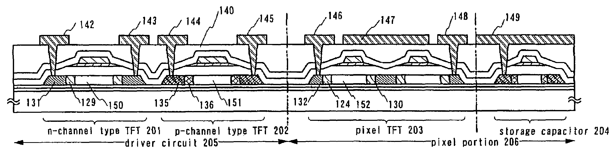
[0060]One embodiment of the present invention is explained below using FIGS. 3A to 5C. A method of manufacturing a pixel portion and driver circuit TFTs (n-channel TFTs and a p-channel TFT), formed in the periphery of the pixel portion, at the same time on the same substrate is explained here in detail.

[0061]In FIG. 3A, aluminum borosilicate glass is used for a substrate 100. A first insulating film is formed on the substrate 100. A 50 nm thick first silicon oxynitride film 101a formed using SiH4, NH3, and N2O as reactant gasses, and a 100 nm thick second silicon oxynitride film 101b formed using SiH4 and N2O as reactant gasses, are laminated in Embodiment 1.

[0062]Semiconductor layers 103 to 106 (for convenience in Embodiment 1, a first semiconductor layer 103, a second semiconductor layer 104, a third semiconductor layer 105, and a fourth semiconductor layer 106) are formed of a semiconductor film 102 having a crystalline structure. The crystalline semiconductor film 10...


PUM


Abstract

The objectives of the present invention are achieving TFTs having a small off current and TFT structures optimal for the driving conditions of a pixel portion and driver circuits, and providing a technique of making the differently structured TFTs without increasing the number of manufacturing steps and the production costs. A semiconductor device has a semiconductor layer, a gate insulating film on the semiconductor layer, and a gate electrode on the gate insulating film. The semiconductor layer contains a channel forming region, a region containing a first concentration impurity element, a region containing a second concentration impurity element, and a region containing a third concentration impurity element. The gate electrode is formed by laminating an electrode (A) and an electrode (B). One edge portion of the electrode (A) overlaps with the region containing the second concentration impurity element, through the gate insulating film, and another edge portion of the electrode (A) overlaps with the channel forming region, through the gate insulating film.

Description

BACKGROUND OF THE INVENTION[0001]1. Field of the Invention[0002]The present invention relates to a semiconductor device using a semiconductor film having a crystalline structure, and to a method of manufacturing the semiconductor device. More specifically, the present invention relates to a semiconductor device having a thin film transistor (TFT) containing an active layer having a channel forming region, a source region, and a drain region from a semiconductor film having a crystalline structure, and a method of manufacturing the semiconductor device.[0003]2. Description of the Related Art[0004]Liquid crystal display devices have widened the marketplace with their advantages of low electric power consumption and space conservation, and have finally reached the point of substituting for CRTs as televisions used daily in households. As such, bright display at high definition equal to or better than that of CRTs, and a price comparable to that of CRTs, are sought for liquid crystal di...

Claims


Application Information

Patent Timeline
Patent Type & Authority Patents(United States)
IPC IPC(8): H01L21/266H01L21/336H01L21/77H01L21/84H01L27/12H01L29/423H01L29/49H01L29/786
CPCH01L29/42384H01L27/124H01L29/66757H01L29/78621H01L29/4908H01L27/12
Inventor NAGAO, RITSUKOHAYAKAWA, MASAHIKO
Owner SEMICON ENERGY LAB CO LTD
Why Eureka
Try Eureka