Substrate processing method and substrate processing apparatus

a substrate processing and substrate technology, applied in the direction of photomechanical equipment, instruments, photosensitive material processing, etc., can solve the problems of inability to completely remove the resist,

Inactive Publication Date: 2005-12-27
TOKYO ELECTRON LTD
View PDF3 Cites 22 Cited by
  • Summary
  • Abstract
  • Description
  • Claims
  • Application Information

AI Technical Summary

Benefits of technology

[0008]The objective of the present invention, developed in consideration of the aforementioned problems, is to

Problems solved by technology

This is because, it is not possible, until now, to completely remove the resist and the polymer only through the application of wet cleaning, utilizing a processing liquid.
However, when dry ashing is conducted

Method used


Image

  • Substrate processing method and substrate processing apparatus
  • Substrate processing method and substrate processing apparatus
  • Substrate processing method and substrate processing apparatus

Examples


Embodiment Construction

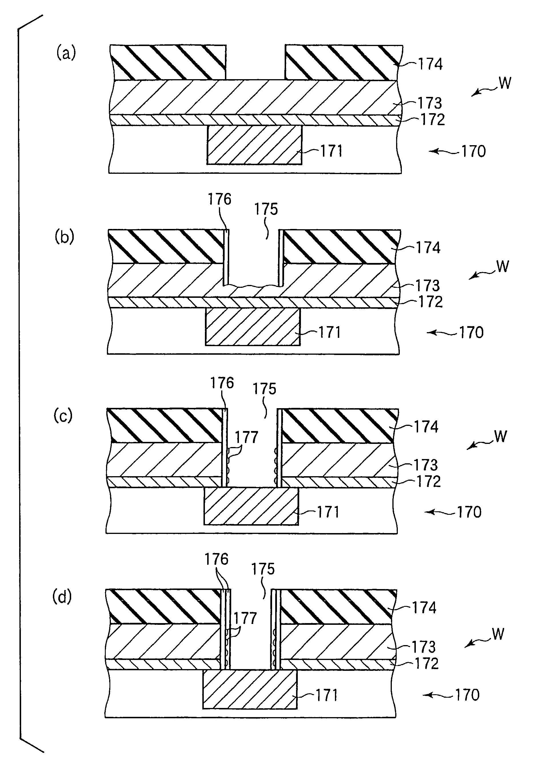
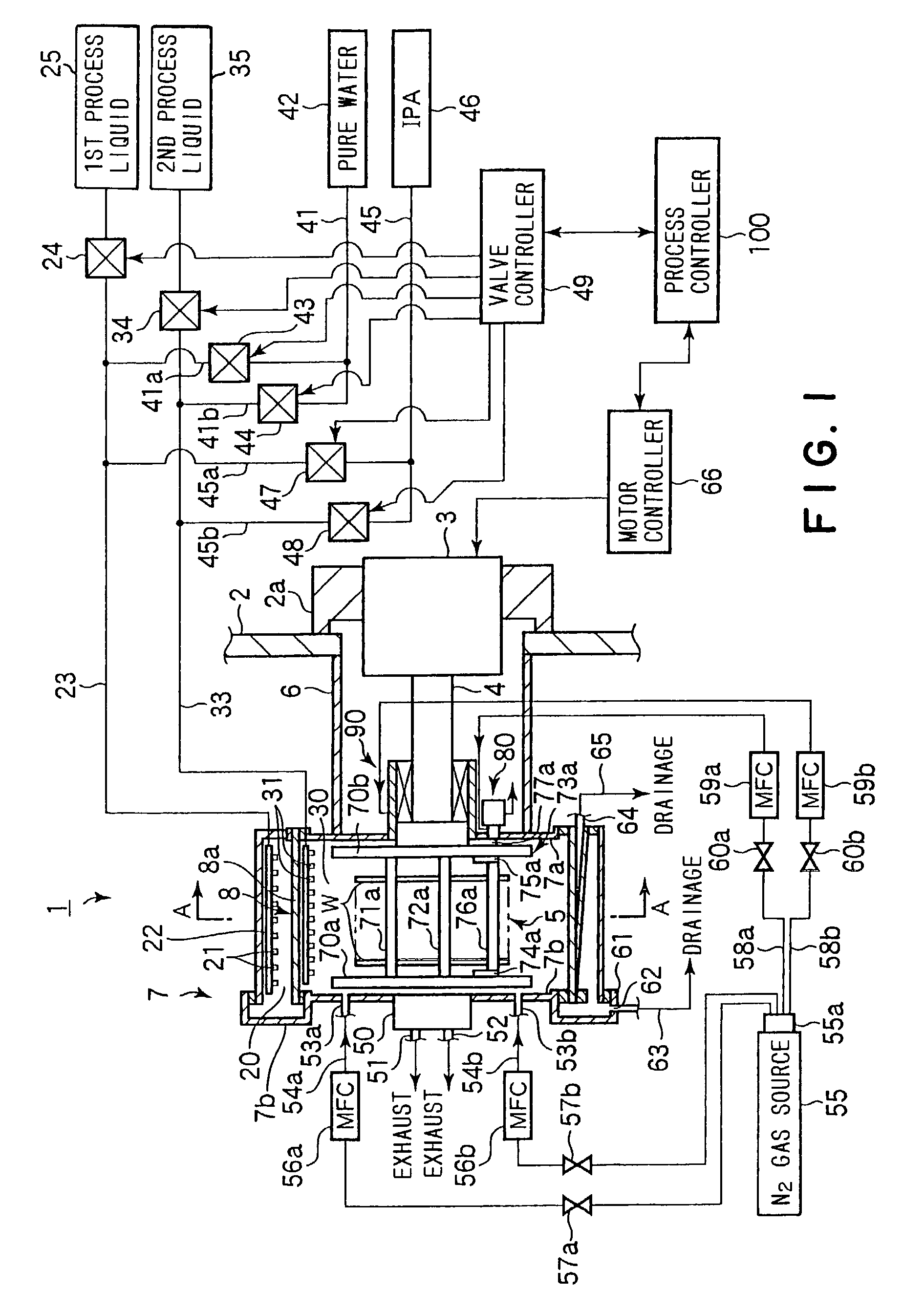
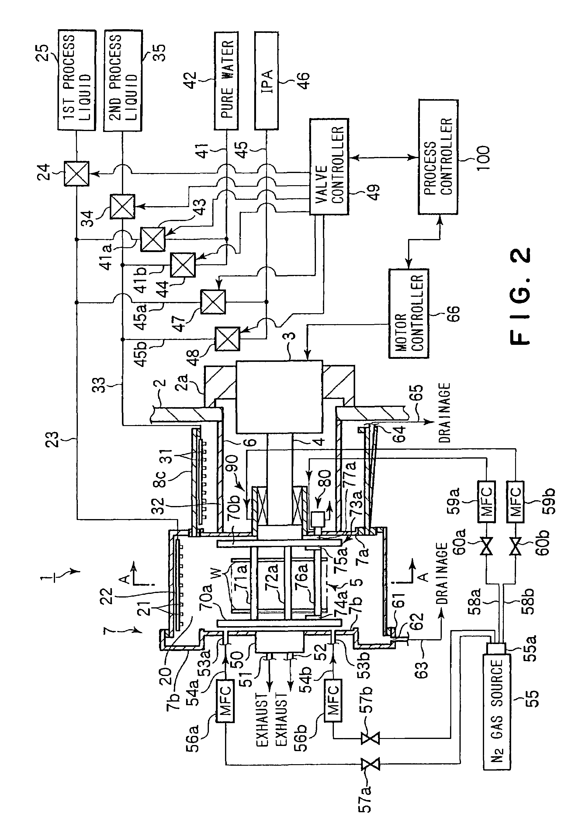
[0025]The processing apparatus 1 according to the present invention is used for the removal of resist layers, polymer layers that are residual of the etching process, and metallic sputter, after the semiconductor wafer (hereinafter referred to as simply “wafer”) W has been subjected to the etching process. As shown in FIGS. 1 thru 3, A motor 3 is affixed to a vertical support wall 2 of the processing apparatus 1 via a support member 2a in such a manner that the revolving shaft 4 of the motor 3 faces a horizontal direction. A rotor 5 is attached to the shaft 4 of the motor 3. A tubular casing 6 extends in a horizontal direction from the support wall 2, and surrounds the motor 3 and the shaft 4. The casing 6 support first enclosure forming members 7 and second enclosure forming members 8 adapted to enclose the rotor 5.

[0026]The rotor 5 is configured to hold a plurality of wafers W (for example 26 pieces) that are stood vertically and aligned in a horizontal direction. The motor 3 rota...


PUM

PropertyMeasurementUnit
Concentrationaaaaaaaaaa
Speedaaaaaaaaaa
Hydrophobicityaaaaaaaaaa

Abstract

A resist film and a polymer layer adhered on a semiconductor substrate can be removed by the method according to the present invention. A first processing liquid, typically including a oxidizing agent, such as hydrogen peroxide solution, is fed to the substrate, thereby the condition of the resist film and the polymer layer is changed. Next, a second processing liquid, typically including a dimethyl sulfoxide and an amine solvent, is fed to the substrate, thereby the resist film and the polymer layer is dissolved and lifted off from the substrate. A sputtered copper particles included in the polymer layer can also be removed.

Description

BACKGROUND OF THE INVENTION[0001]1. Field of the Invention[0002]This invention relates to a substrate processing apparatus and substrate processing method for removing, utilizing a processing liquid, adhesives such as resist, polymers, etc., which adhere to the substrate during the process of the substrate, such as semiconductor device manufacturing process.[0003]2. Description of the Related Art[0004]Recently, in the process of manufacturing semiconductor devices, the miniaturization of design rules has rapidly progressed. Along with this has come the use of a low-dielectric-constant organic film as an interlayer insulating film called low-k film, and the use of Cu having low electrical resistance as a wiring-layer material instead of Al, in view of the high speed operation of the semiconductor devices.[0005]Dual damascene process has been utilized to form Cu wiring layers with the interlayer insulating film being arranged between the adjacent Cu wiring layers. The dual damascene p...

Claims


Application Information

Patent Timeline
IPC IPC(8): G03F7/42H01L21/304H01L21/027H01L21/302H01L21/306H01L21/311H01L21/461
CPCG03F7/422H01L21/02063H01L21/31133H01L21/31138H01L21/67017H01L21/67028H01L21/76814H01L21/304
Inventor NIUYA, TAKAYUKIORII, TAKEHIKOMORI, HIROYUKIYANO, HIROSHINAKAMORI, MITSUNORI
Owner TOKYO ELECTRON LTD
Why Eureka
Try Eureka