Supercharge Your Innovation With Domain-Expert AI Agents!

In-line program system for assembly printed circuit board

a printed circuit board and program system technology, applied in the field of parallel automated programming of programmable electronic devices, can solve the problem that the pcba designer is not restricted in the choice of pics, and achieve the effect of faster production speed, higher quality and faster pa

Inactive Publication Date: 2006-01-10
BP MICROSYST
View PDF12 Cites 18 Cited by
  • Summary
  • Abstract
  • Description
  • Claims
  • Application Information

AI Technical Summary

Benefits of technology

[0011]The present invention addresses all of the above problems (e.g., costs, complications and delays) by performing the programming and testing operations with the same piece of equipment that performs the assembly operation. Using the techniques of the present invention, PICs are programmed on demand so the need for an inventory of programmed PICs is eliminated, and changes to the program pattern may be incorporated immediately without waste. Any PICs that fail to program are rejected by the ILP system so that bad PICs are never placed onto a PCBA. Because the PCBA does not have to be designed to accommodate an in-circuit programming technique, the PCBA designer is unconstrained in choice of PICs. The ILP system generally programs PICs faster than PICs can be programmed using the in-circuit programming methodology. The ILP system is also able to program a number of devices simultaneously, allowing a PCBA assembly line to produce PCBAs at a faster pace than that at which a single PIC can be programmed. Thus, an assembly line incorporating an ILP system may be smaller and produce PCBAs faster, with higher quality and less expense than an assembly line incorporating an in-circuit programming system. Further, the use of an ILP system in an assembly line allows for PCBAs to be produced less expensively than in an assembly line incorporating programmed PICs from an off-line programming system.

Problems solved by technology

Because the PCBA does not have to be designed to accommodate an in-circuit programming technique, the PCBA designer is unconstrained in choice of PICs.

Method used


Image

  • In-line program system for assembly printed circuit board
  • In-line program system for assembly printed circuit board
  • In-line program system for assembly printed circuit board

Examples


Embodiment Construction

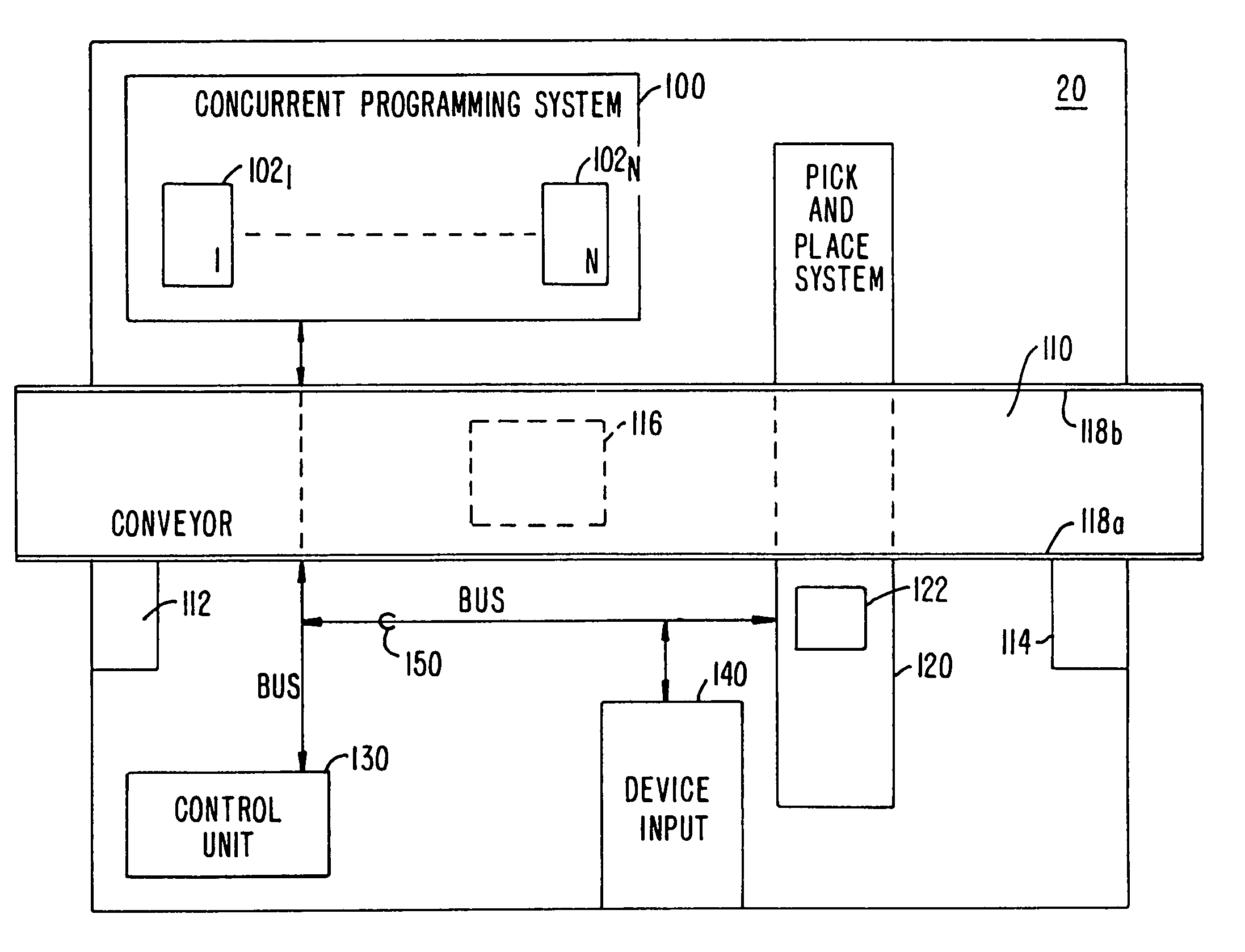
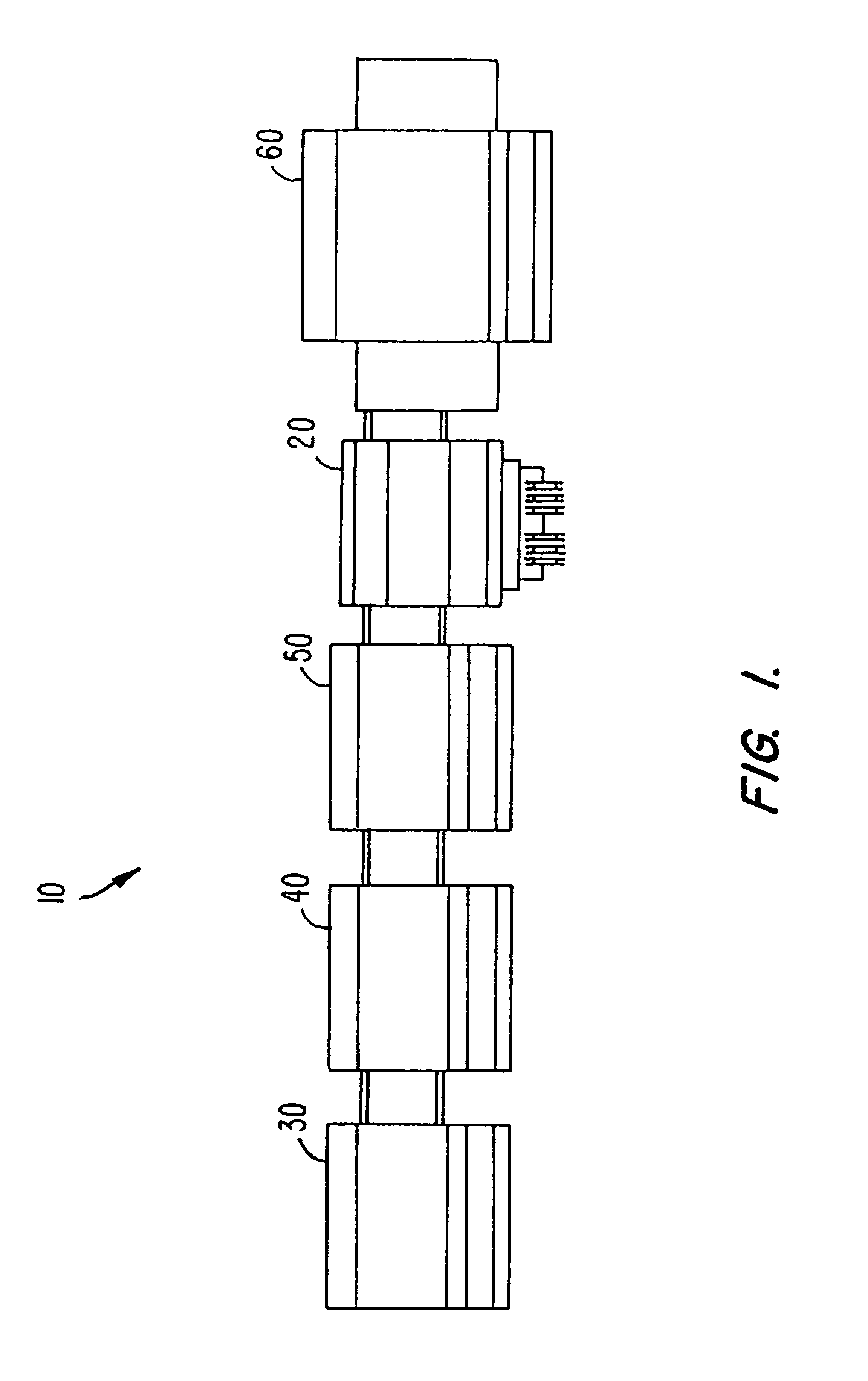
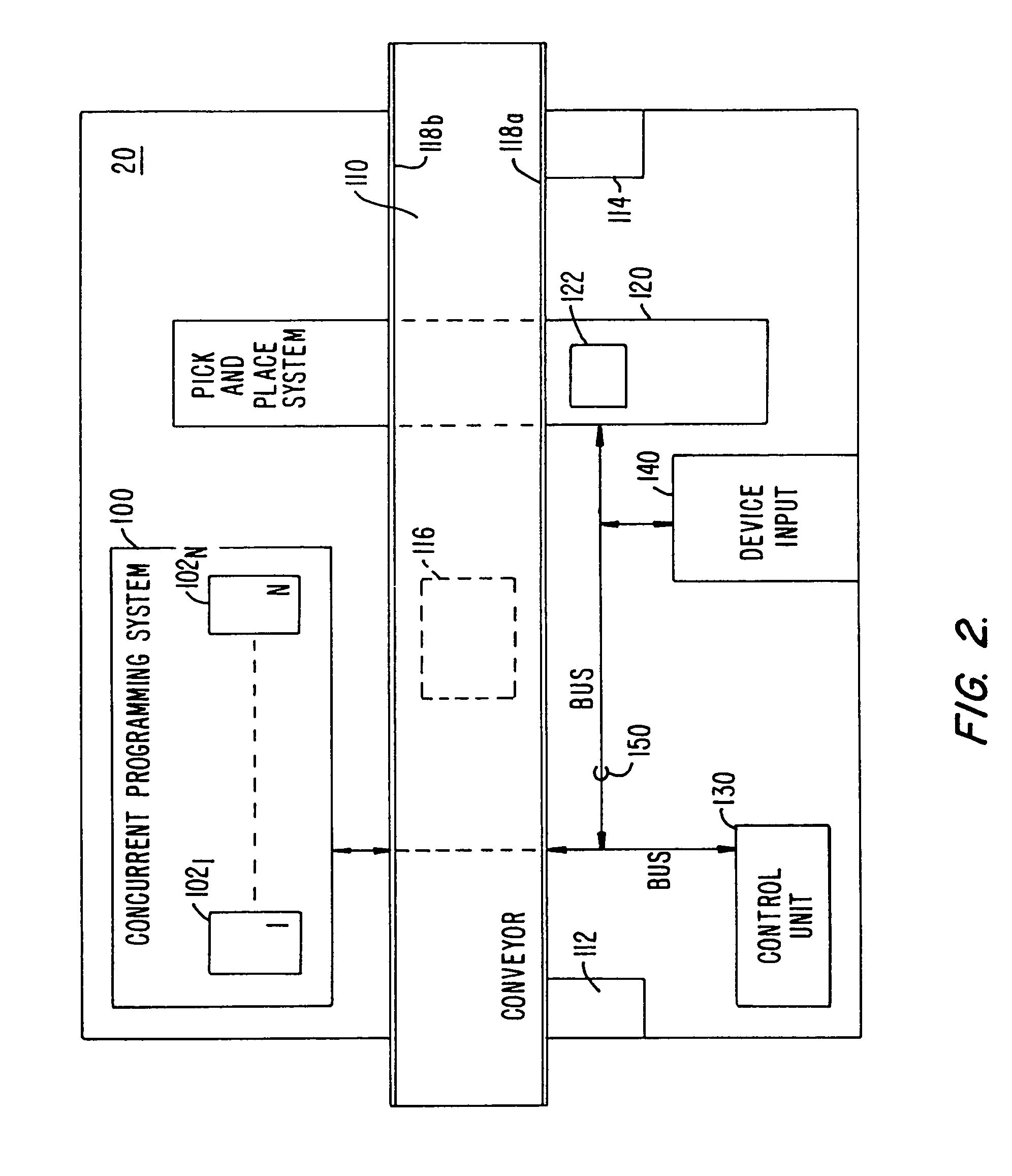
[0021]FIG. 1 illustrates a block diagram view of a surface mount production line 10 including an inline programming apparatus 20 according to an embodiment of the present invention. As shown, surface mount production line 10 includes a linear array of machines or components that perform unique functions. For example, component 30 may be a stencil printer machine 30 that controls the application of solder paste to a blank circuit board. Component 40 may be a chip shooter machine that performs high speed placement of devices and circuit elements that do not require a high level of placement accuracy. Such devices and elements include resistors, capacitors, and the like. Component 50 may be a fine pitch placement machine that places devices at low speed with extreme accuracy. Component 60 may be a reflow oven that “cooks” the solder paste, thereby soldering to the board all the devices and elements that were placed on the board by the previous machines. Each component of production lin...


PUM


Abstract

An in-line programming (ILP) system and method for programming and testing programmable integrated circuit devices (PICs) and performing the assembly of printed circuit board assemblies (PCBAs). Printed circuit boards enter and leave the ILP system on a conveyor system. PICs are loaded into the ILP system, and the ILP system automatically programs and tests the PICs and places them onto the PCBs as the PCBs arrive on the conveyor. The programming and testing operations are performed by the same piece of equipment that performs the PCBA assembly operation.

Description

CROSS REFERENCES TO RELATED APPLICATIONS[0001]This application is a divisional of U.S. patent application Ser. No. 09 / 776,095, filed Feb. 1, 2001 now U.S. Pat. No. 6,687,986, which is a continuation of U.S. patent application Ser. No. 09 / 493,953, filed Jan. 28, 2000, now U.S. Pat. No. 6,230,067, entitled “In-Line Programming System and Method,” which is related to U.S. Provisional Patent Application Ser. No. 60 / 117,873 filed Jan. 29, 1999, entitled “N-LINE PROGRAMMING DEVICE WITH SELF TEACHING CAPACITY,” and the disclosures of each are hereby incorporated by reference.BACKGROUND OF THE INVENTION[0002]The present invention generally relates to concurrent automated programming of programmable electronic devices, and more particularly to programming and testing multiple device types and patterns and performing circuit board assembly simultaneously in a single in-line programming device.[0003]In the semiconductor industry, a considerable number of electronic devices such as programmable...

Claims


Application Information

Patent Timeline
IPC IPC(8): B23P19/00G01R31/28H05K13/04G06F19/00H05K3/30
CPCH05K13/04H05K13/08G01R31/2808Y10T29/49139Y10S414/135Y10T29/53091Y10T29/4913Y10T29/53048Y10T29/49144Y10T29/49004Y10T29/53178Y10T29/5196Y10T29/53022Y10T29/53187Y10T29/53013Y10T29/53174H05K13/085H05K13/0857
Inventor WHITE, WILLIAM H.
Owner BP MICROSYST
Features
  • R&D
  • Intellectual Property
  • Life Sciences
  • Materials
  • Tech Scout
  • Unparalleled Data Quality
  • Higher Quality Content
  • 60% Fewer Hallucinations
Learn More