

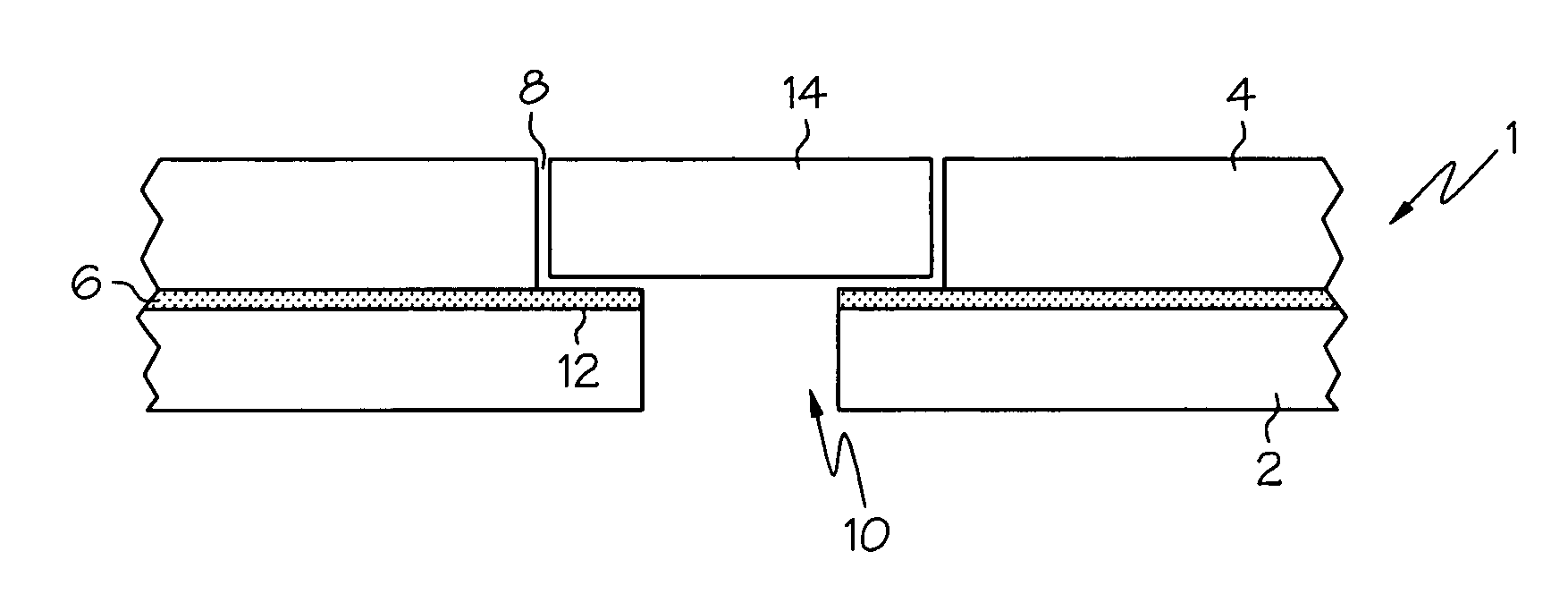
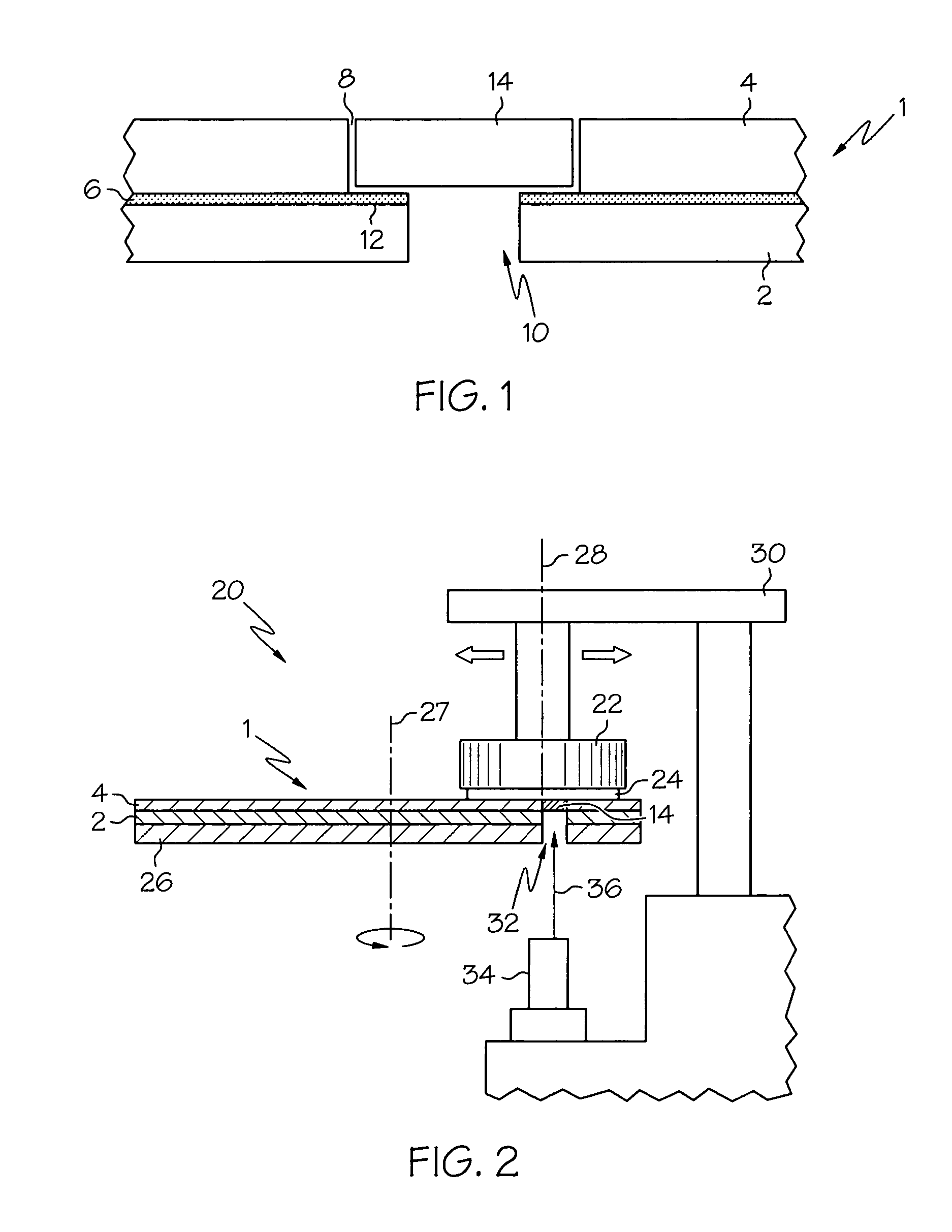
Polishing pad with high optical transmission window
a technology of optical transmission window and polishing pad, which is applied in the field of polishing pads, can solve the problems of difficult in-situ robust steep decline to about 13%, and difficult hammer effective endpoint detection or measurement for a wide variety of reasons
- Summary
- Abstract
- Description
- Claims
- Application Information
AI Technical Summary
Benefits of technology
Problems solved by technology
Method used
Image

Examples
examples
[0024]In the Examples, numerals represent examples of the invention and the letter represents a comparative example. In this experiment, the percent optical transmission for exemplary windows of the present invention was measured using a Gretag Macbeth 3000A spectrophotometer, for the wavelength range of 360 nm to 750 nm. In particular, windows formed from aliphatic diisocyanate-containing materials were tested against a window formed from an aromatic diisocyanate-containing material. For Test A, 100 parts of the prepolymer kept at 120° F., with 26 parts of the curing agent kept at 240° F., was mixed in a liquid tank and degassed under vacuum (<1 torr). The mixture was then cast in a mold and cured at 220° F. for 18 hours. For Tests 1–8, 100 parts of the prepolymer kept at 150° F., with appropriate amounts of the curing agent kept at room temperature, was mixed in a liquid tank and degassed under vacuum (<1 torr). The mixture was then cast in a mold and cured at 220° F. for 18 hours...
PUM
| Property | Measurement | Unit |
|---|---|---|
| wavelength range | aaaaa | aaaaa |
| wavelength | aaaaa | aaaaa |
| temperature | aaaaa | aaaaa |
Abstract
Description
Claims
Application Information