Methods for making copper and other metal interconnections in integrated circuits

a technology of interconnection and copper, which is applied in the direction of semiconductor devices, semiconductor/solid-state device details, electrical apparatus, etc., can solve the problems of promoting the consolidation of the copper within the trench or hole. , to achieve the effect of reducing the electrical resistance, increasing the cross-sectional area of the conductor, and eliminating not only the time-consuming step

Inactive Publication Date: 2006-01-10
MICRON TECH INC
View PDF68 Cites 51 Cited by
  • Summary
  • Abstract
  • Description
  • Claims
  • Application Information

AI Technical Summary

Benefits of technology

[0013]The preferred embodiment provides at least two advantages over the Hirao and related techniques. First, in contrast to conventional magnetron sputtering, ionized-magnetron sputtering of the first material and the conductor metal forms a trench lining and a metal conductor that more accurately conforms to the trench profile, thus increasing cross-sectional area of the conductor and ult

Problems solved by technology

Moreover, after filling the trench or hole with copper, the preferred method heats, or anneals, the copper-filled trench, thereby promoting voidless consolidation of the copper within the trench or hole.
First, in contrast to conventional magnetron sputtering, ionized-

Method used


Image

  • Methods for making copper and other metal interconnections in integrated circuits
  • Methods for making copper and other metal interconnections in integrated circuits
  • Methods for making copper and other metal interconnections in integrated circuits

Examples


Embodiment Construction

[0025]The following detailed description, which references and incorporates FIGS. 1-8, describes and illustrates one or more specific embodiments of the invention. These embodiments, offered not to limit but only to exemplify and teach the invention, are shown and described in sufficient detail to enable those skilled in the art to practice the invention. Thus, where appropriate to avoid obscuring the invention, the description may omit certain information known to those of skill in the art.

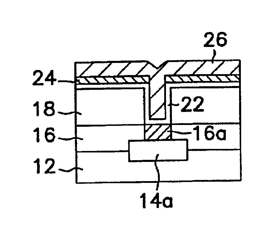
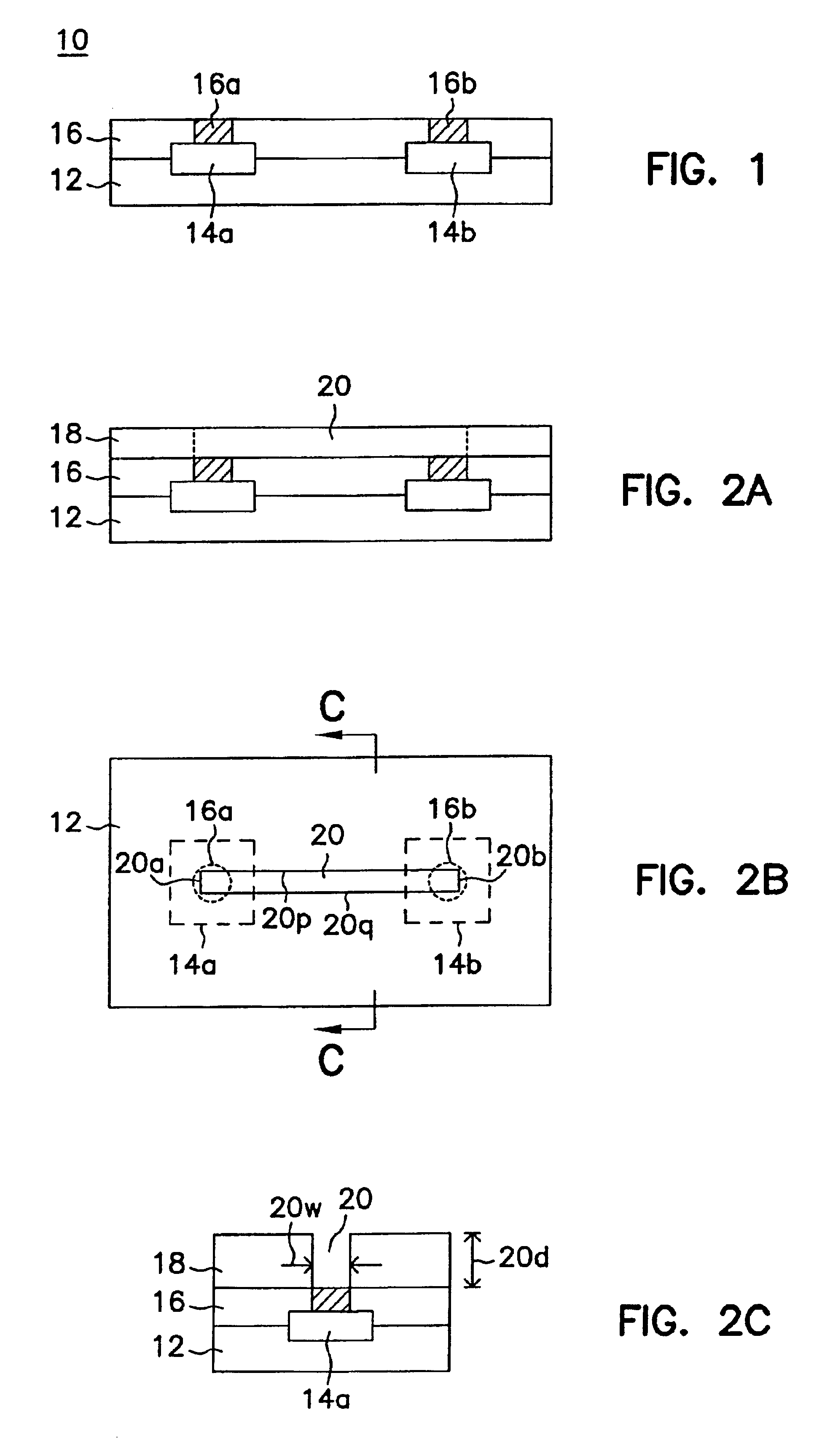
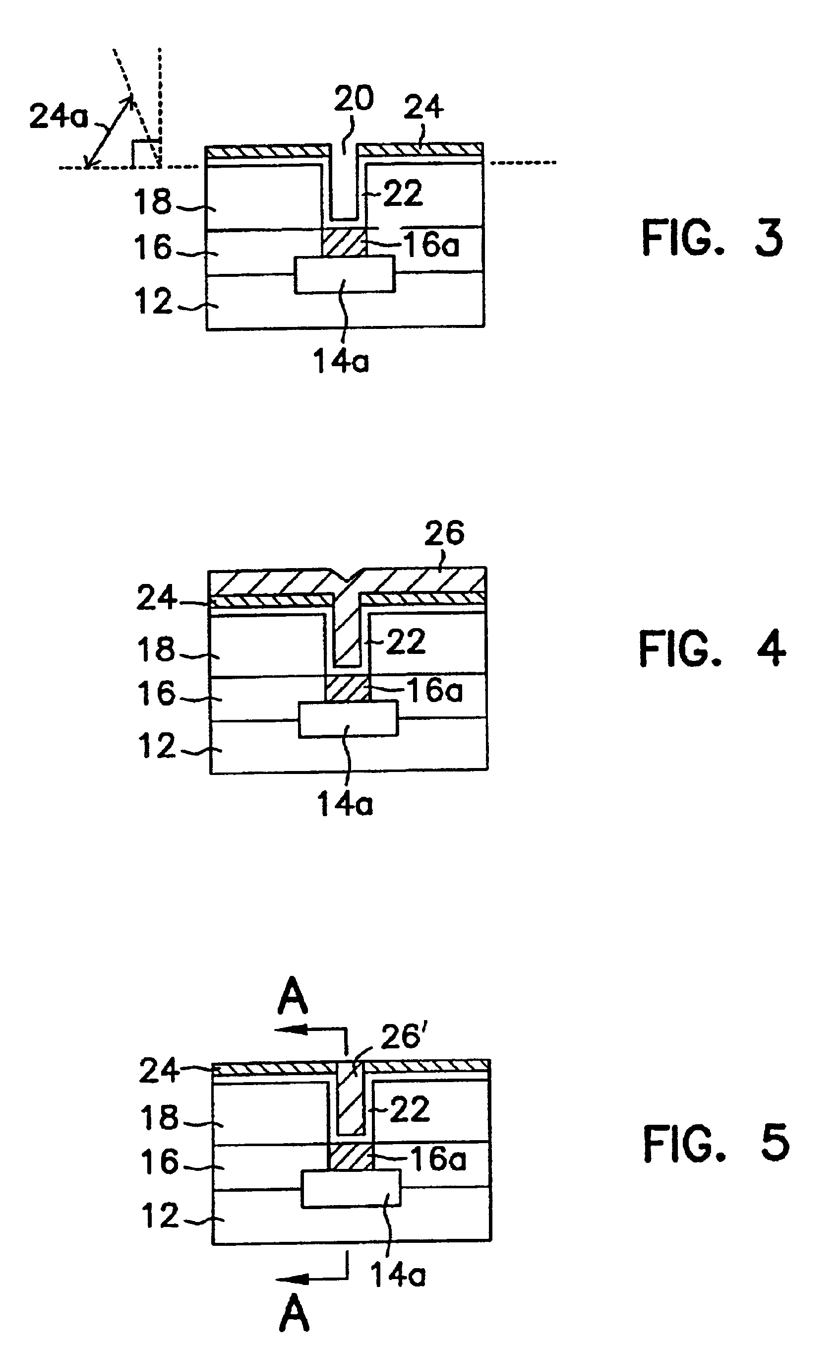
[0026]FIGS. 1-8 show a number of preferred integrated-circuit assemblies, which taken collectively and sequentially, illustrate the preferred method of the present invention. The method, as shown in FIG. 1, begins with a known integrated-circuit assembly or structure 10, which can be within any integrated circuit, a dynamic-random-access memory, for example. Assembly 10 includes a substrate 12. The term “substrate,” as used herein, encompasses a semiconductor wafer as well as structures having on...


PUM


Abstract

A typical integrated-circuit fabrication requires interconnecting millions of microscopic transistors and resistors with aluminum wires. Yet, aluminum wires have greater electrical resistance and are less reliable than copper wires. Unfortunately, current techniques for making copper wires are time-consuming and inefficient. Accordingly, the invention provides a method of making wires or interconnects from copper or other metals. One embodiment entails forming a first diffusion barrier inside a trench using ionized-magnetron sputtering for better conformal coating of the trench, and a second diffusion barrier outside the trench using jet-vapor deposition. The jet-vapor deposition has an acute angle of incidence which prevents deposition within the trench and thus eliminates conventional etching steps that would otherwise be required to leave the trench free of this material. After formation of the two diffusion barriers, the trench is filled with metal and annealed.

Description

[0001]This application is a Divisional of U.S. application Ser. No. 09 / 032,197, filed Feb. 27, 1998 now U.S. Pat. No. 6,211,073.FIELD OF INVENTION[0002]The present invention concerns methods of semiconductor device or integrated circuit manufacturing, particularly methods of forming interconnects from copper and other metals.BACKGROUND OF THE INVENTION[0003]Integrated circuits, the key components in thousands of electronic and computer products, are interconnected networks of electrical components fabricated on a common foundation, or substrate. Fabricators typically use various techniques, such as layering, doping, masking, and etching, to build thousands and even millions of microscopic resistors, transistors, and other electrical components on a silicon substrate, known as a wafer. The components are then “wired,” or interconnected, together to define a specific electric circuit, such as a computer memory.[0004]Interconnecting millions of microscopic components typically entails ...

Claims


Application Information

Patent Timeline
IPC IPC(8): H01L23/52H01L21/4763H01L21/768H01L23/532
CPCH01L21/76834H01L21/76843H01L21/76877H01L23/53238H01L2924/0002H01L2924/00
Inventor AHN, KIE Y.FORBES, LEONARD
Owner MICRON TECH INC
Why Eureka
Try Eureka