Bonding pad structure of a semiconductor device

a technology of bonding pad and semiconductor device, which is applied in the direction of semiconductor device, semiconductor/solid-state device details, electrical apparatus, etc., can solve the problems of many additional fabrication process steps for implementation, and achieve the effect of improving the bonding and improving the distribution of physical stresses on the bonding pad

Inactive Publication Date: 2006-01-10
SAMSUNG ELECTRONICS CO LTD
View PDF16 Cites 15 Cited by
  • Summary
  • Abstract
  • Description
  • Claims
  • Application Information

AI Technical Summary

Benefits of technology

[0010]According to embodiments of the present invention, a bonding pad structure in an integrated circuit (IC) and a method for manufacturing thereof preferably comprise a plurality of dummy patterns being deposited in sub-layers of the IC and then being connected via a metal link to a plurality of complementary top surface bonding pads during the same process steps performed to construct the circuit elements of the IC, thereby minimizing or eliminating additional or special process steps required in conventional techniques. Such an imbedded anchoring structure provides improved resistance to layer de-lamination during pulling stresses associated with conventional wire bonding operations and normal mechanical stresses associated with chip-on-chip applications.
[0011]The anchoring structure in a semiconductor IC having a plurality of electrical devices and a plurality of deposition layers, preferably comprises a bonding pad having a first interconnection layer and a second interconnection layer integral to each other and at least one peg that vertically traverses at least a portion of one or more intervening deposition layers of the IC. The anchoring structure provides improved bonding between deposition layers as well as improved distribution of physical stress on the bonding pad. The pegs may or may not be electrically conductive, and may or may not be composed of a metal material. When metal is used as the bonding pad material in the embodiments of the present invention, such metal may be preferably selected from a group consisting of tungsten, aluminum, copper and nickel.
[0012]The structure may include a bottom surface area of the bonding pad and at least one peg that comprises an area sufficient to: 1) preserve the physical integrity of the semiconductor IC, or 2) prevent de-lamination of the bonding pad from the semiconductor IC. A plurality of pegs may be formed in a mesh type pattern that is integral with the bonding pad.
[0023]A preferred embodiment of a bonding pad structure in a semiconductor IC having a plurality of electrical devices and a plurality of deposition layers, preferably comprises: a metallic bonding pad having at least a first interconnection layer and a second interconnection layer, which are bonded to each other by a peg vertically traversing at least a portion of one or more intervening deposition layers therebetween, so as to provide improved binding between the plurality of deposition and interconnection layers and thus provide improved distribution of physical stresses on the bonding pad. The metal is preferably electrically conductive, such as tungsten, aluminum, copper and nickel. In a preferred embodiment, a plurality of pegs form a mesh type pattern that is integral with the bonding pad.

Problems solved by technology

A significant disadvantage, however, is that the polysilicon layer is typically deposited directly over a layer of insulating material rather than over a layer of a metallic material, thereby providing adhesion and anchoring characteristics that are not optimal.
A significant disadvantage of such approaches is that they require many additional fabrication process steps for implementation, rather than fabricating the bonding pad anchoring structure simultaneous with other circuit element processing steps.

Method used


Image

  • Bonding pad structure of a semiconductor device
  • Bonding pad structure of a semiconductor device
  • Bonding pad structure of a semiconductor device

Examples


first embodiment

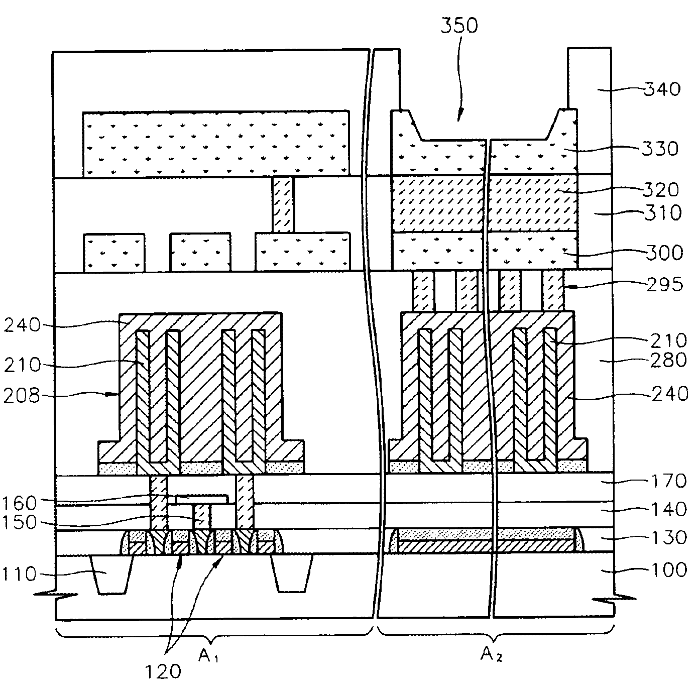
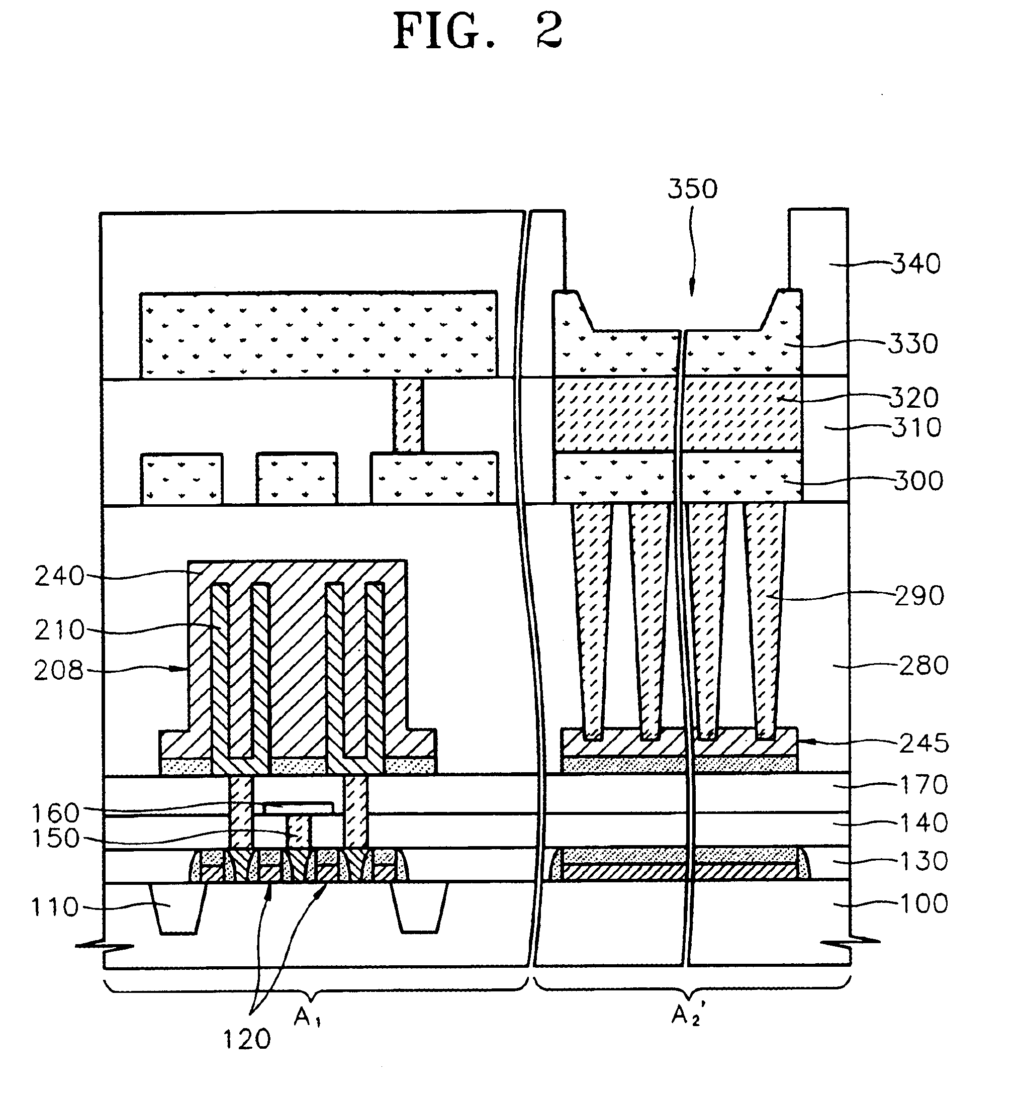
[0062]FIG. 2 illustrates a bonding pad structure according to the present invention. An IC memory cell A1 comprising a capacitor 208 having electrodes 210 and 240 may be included in a first, a second, a third, and a fourth dielectric layers, 130, 140, 170, and 280, respectively.

[0063]The bonding pad structure is created beneath and connected to a bonding pad 350 simultaneously with the processing of the capacitor 208 of memory cell A1. Anchoring elements of the bonding pad structure preferably comprises a dummy pattern 245 being formed on the third interlayer dielectric 170, which is conductively and mechanically connected by a plurality of plugs 290 through interlayer dielectric 280 to a lower portion of a multi-layered bonding pad 350, and more specifically, to a first aluminum interconnection layer 300.

[0064]In order to connect first aluminum interconnection layer 300 to the dummy pattern 245, contact holes are formed in interlayer dielectric 280 in a bonding pad region A2′ to th...

second embodiment

[0083] as shown in the processing of bonding pad region A2″ in FIGS. 4-1 through 4-18, smaller depth of a bonding pad contact hole allows for easier and more uniform formation of both the bonding pad contact holes and the tungsten filler plugs 295. As was shown in the preceding steps for bonding pad region A2′, the dummy patterns under the bonding pads may be easily formed at the same time and during the same process steps that were used for the construction of the capacitor, i.e. without the need of extra process steps, or at most a minimum number of additional steps.

[0084]FIG. 5 illustrates a bonding pad structure according to a third embodiment of the present invention. In the embodiment illustrated in FIG. 5, a trench is not formed in the second interlayer dielectric 140, unlike in the second embodiment. In this embodiment, a capacitor pattern may be constructed beneath the bonding pad 350 for use as a dummy pattern, rather than the dummy pattern in trench 155 of FIG. 4-3, there...

fourth embodiment

[0086]FIG. 6 illustrates a bonding pad structure according to the present invention. In this embodiment, a tungsten plug 355 (or plugs) may have a rectangular-shaped, wedge-shape, or even solid cubic-shaped characteristics. The selection of a particular shape and or depth of a plug 355 is related to a design selection regarding the materials and complexity of the construction vs. the advantages obtained. Such advantages may relate to the reliability of the structure or some other electronic or mechanical performance parameter, such as current-carrying capability or mechanical flexibility.


PUM


Abstract

A bonding pad structure in an integrated circuit (IC) and a method for manufacturing thereof comprises a plurality of dummy patterns deposited in sub-layers of the IC, each dummy pattern being connected via a metal link to a plurality of complementary top surface bonding pads, wherein the dummy patterns and the metal link are constructed during the same process steps used to construct the circuit elements included in the IC, without additional or special process steps. Such an imbedded and anchored bonding pad provides contact reliability for both conductive and non-conductive pads used for the interconnection of integrated circuits in a manner that resists layer separation or de-lamination under pulling stresses that are present on the bonding pads.

Description

BACKGROUND OF THE INVENTION[0001]1. Field of the Invention[0002]The present invention relates to the manufacture of semiconductor devices and, more particularly, to a structure directed to and a method for creating a de-lamination resistant interconnection bonding pad in a semiconductor device.[0003]2. Description of the Related Art[0004]A bonding pad connects an integrated circuit on a chip to an integrated circuit outside the chip. FIG. 1 illustrates a cross-sectional view of a conventional semiconductor memory device having a device isolation region 110, a bonding pad 350 for communicating signals externally to the chip, and a DRAM (dynamic random access memory) cell having a stack capacitor and a switching transistor 120. In FIG. 1, A1 represents a memory cell region, and A2 represents a bonding pad region. Reference numeral 120 represents a switching transistor in memory cell region A1, and reference numerals 130,140, 170 and 280 represent interlayer dielectric layers. Referenc...

Claims


Application Information

Patent Timeline
Patent Type & Authority Patents(United States)
IPC IPC(8): H01L23/48H01L23/52H01L29/40H01L21/3205H01L21/60H01L21/8242H01L23/485H01L23/58H01L27/108
CPCH01L23/585H01L24/05H01L27/10894H01L27/10897H01L24/03H01L2924/01072H01L27/10814H01L27/10817H01L2224/05082H01L2224/05093H01L2224/05124H01L2224/05556H01L2224/05624H01L2924/01004H01L2924/01005H01L2924/01006H01L2924/01013H01L2924/01014H01L2924/01015H01L2924/01028H01L2924/01029H01L2924/01074H01L2924/01075H01L2924/01082H01L2924/01327H01L2924/05042H01L2924/14H01L2924/19041H01L2924/19043H01L2924/01068H01L2924/01033H01L2924/01023H01L2924/01019H01L2924/00014H10B12/315H10B12/318H10B12/09H10B12/50H01L21/60
Inventor CHO, TAI-HEUIKANG, HYUCK-JINKIM, MIN-CHULKIM, BYUNG-YOON
Owner SAMSUNG ELECTRONICS CO LTD
Why Eureka
Try Eureka