Method of forming printed circuit card

a technology of printed circuit cards and circuit boards, applied in the field of circuit boards or cards, can solve the problems of affecting the appearance of printed circuit boards,

Inactive Publication Date: 2006-01-17
INT BUSINESS MASCH CORP
View PDF17 Cites 6 Cited by
  • Summary
  • Abstract
  • Description
  • Claims
  • Application Information

AI Technical Summary

Problems solved by technology

While photoimageable material has been used on one side of a metal substrate, various processing difficulties are encountered when using photoimageable material to form a 2S / 1P board, with the photoimageable material on both sides of the metal power plane.
If the same process were used after the copper is etched away, the parts of the panel would be isolated and would literally fall apart since there is no remaining material to hold them together.

Method used


Image

  • Method of forming printed circuit card
  • Method of forming printed circuit card
  • Method of forming printed circuit card

Examples


Embodiment Construction

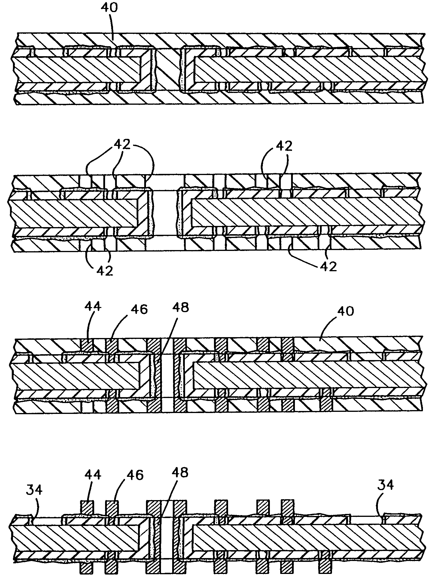
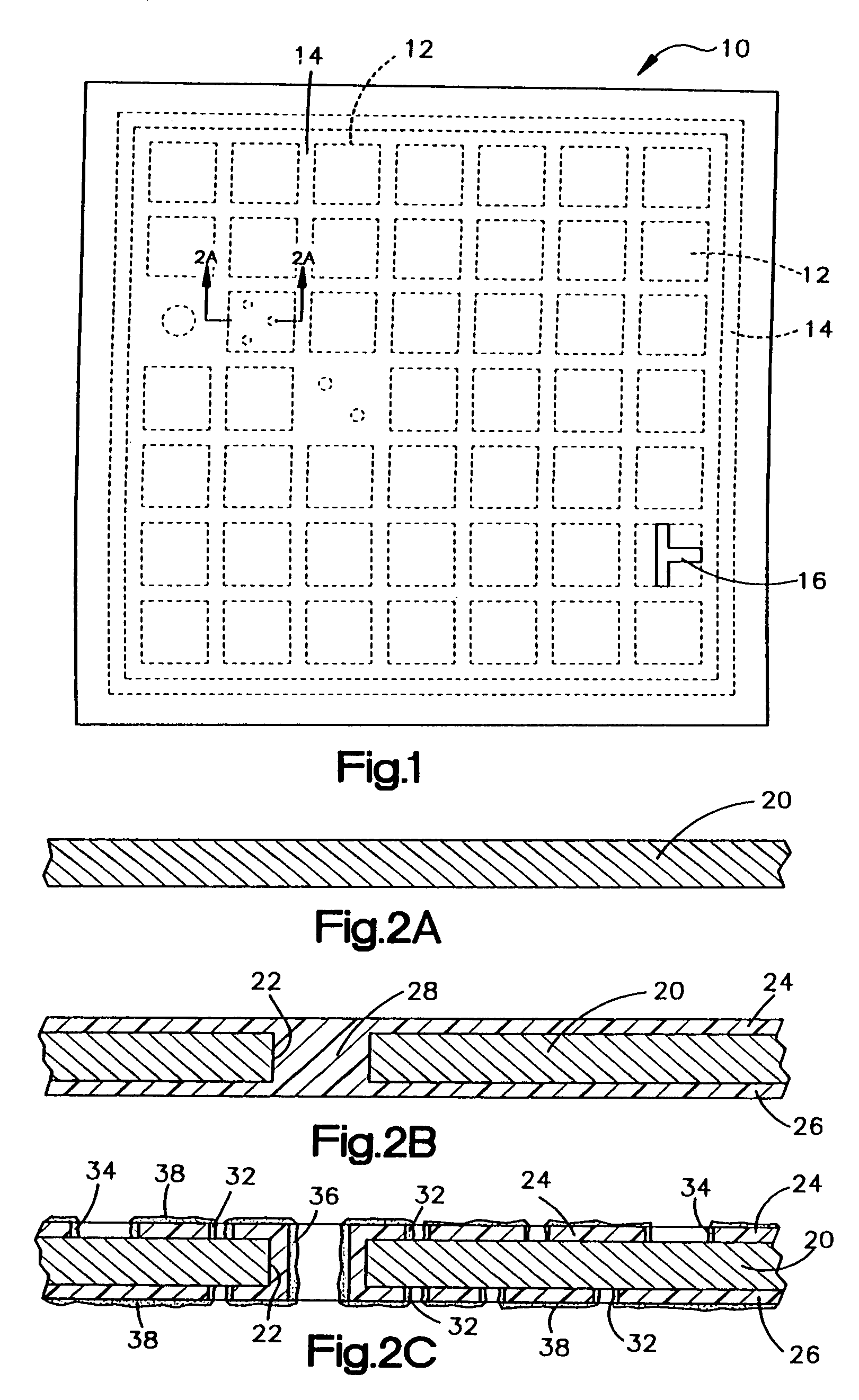
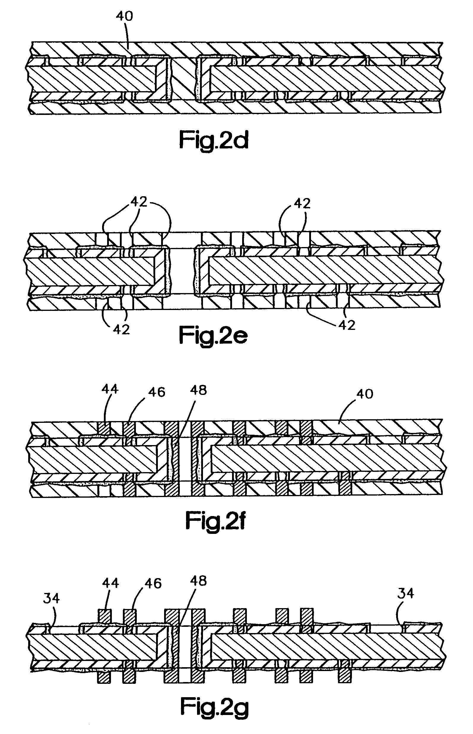
[0011]Referring now to the drawings, FIG. 1 shows a very schematic representation of a panel used to form a plurality of circuit cards or boards thereon when the cards, boards or sections of cards or boards are required to be electrically separated, i.e., there can be no physical contact in the power plane between the various cards or boards being formed. As shown in FIG. 1, panel 10 has a plurality of circuit cards designated by the reference character 12 formed thereon, and the various cards 12 are separated by borders 14 which extend completely around each of the cards 12. Borders 16 are borders that provide an electrical separation within a card. The term “cards” or “circuit cards” is used herein to designate circuitized substrates which can be used as chip carriers, or circuit boards for the mounting of components as well as chips. The formation of the cards 12 is shown in the various stages thereof in FIGS. 2A–2k starting with a metal layer which will form the power plane and ...


PUM

PropertyMeasurementUnit
thickaaaaaaaaaa
thickaaaaaaaaaa
thickaaaaaaaaaa

Abstract

A method of forming a printed circuit card with a metal power plane layer between two photoimageable dielectric layers is provided. Photoformed metal filled vias plated through holes are in the photopatternable material, and signal circuitry is on the surfaces of each of the dielectric materials connected to the vias and plated through holes. A border may be around the card including a metal layer termination in from the edge of one of the dielectric layers. Copper foil with clearance holes is provided. First and second layers of photoimageable curable dielectric material are on opposite sides of the copper. Patterns are developed on the first and second layers of the photoimageable material to reveal the metal layer through vias. Through holes are developed where holes were patterned in both dielectric layers. The surfaces of the photoimageable material, vias and through holes are metallized by copper plating, preferably using photoresist.

Description

CROSS REFERENCE TO RELATED APPLICATIONS[0001]This application is a division of patent application Ser. No. 09 / 690,485 filed Oct. 17, 2000, which is U.S. Pat. No. 6,750,405 which is a continuation of application Ser. No. 09 / 203,956 filed Dec. 2, 1998, which is U.S. Pat. No. 6,204,453 B1, which, in turn, is a continuation-in-part of application Ser. No. 08 / 774,849 filed Dec. 27, 1996, which is U.S. Pat. No. 5,876,842, which is a continuation of application Ser. No. 08 / 486,822 filed Jun. 7, 1995, now abandoned.BACKGROUND OF THE INVENTION[0002]This invention relates generally to the formation of circuit boards or cards or the like, and more particularly to the formation of circuit boards or cards having two signal planes and one power plane (2S / 1P) wherein the power plane is sandwiched between two layers of photopatternable dielectric material and on which layers of circuitry for the signal planes are disposed.BACKGROUND INFORMATION[0003]In certain conventional circuit board configurati...

Claims


Application Information

Patent Timeline
Patent Type & Authority Patents(United States)
IPC IPC(8): H05K3/36H01L23/498H01L23/50H05K1/05H05K1/11H05K3/00H05K3/10H05K3/42H05K3/44H05K3/46
CPCH01L23/49827H01L23/50H05K1/113H05K3/429H05K3/44H05K3/445H05K3/4641H01L23/49833Y10T29/49155H05K1/056H05K3/0023H05K3/0052H05K3/0094H05K3/06H05K3/108H05K3/426H05K3/4623H05K2201/0919H05K2201/09536H05K2201/09554H05K2201/096H05K2201/10734H05K2203/0323H05K2203/0574H05K2203/0733H05K2203/1394H01L2924/0002Y10T29/49126Y10T29/49156Y10T29/49165Y10T29/49128Y10T29/49117H01L2924/00
Inventor FALLON, KENNETHJIMAREZ, MIGUEL A.KEESLER, ROSS W.LAUFFER, JOHN M.MAGNUSON, ROY H.MARKOVICH, VOYA R.MEMIS, IRVPAOLETTI, JIM P.PERRINO, MARYBETHWELSH, JOHN A.WILSON, WILLIAM E.
Owner INT BUSINESS MASCH CORP
Why Eureka
Try Eureka