Optical connection device

a technology of optical connection and optical pin, which is applied in the direction of optical elements, semiconductor lasers, instruments, etc., can solve the problems of increasing the distance between the wires, the interference of signals between the wiring circuit and the propagation delay caused by the increase in the wiring distance, and the difficulty of optical coupling, etc., to achieve efficient coupling with the optical waveguide

Inactive Publication Date: 2006-01-17
NIPPON SHEET GLASS CO LTD +1
View PDF4 Cites 77 Cited by
  • Summary
  • Abstract
  • Description
  • Claims
  • Application Information

AI Technical Summary

Benefits of technology

[0024]Preferably, a light-condensing unit represented by a lens may be interposed at least between the light-emitting element and the optical unit. Light emitted from the light-emitting element is generally divergent light. When the light-condensing unit is used,

Problems solved by technology

However, problems such as interference of signals between wiring circuits and propagation delay caused by increase in wiring distance are growing more serious.
Optical coupling, however, needs precise positioning (alignment) and is not easy compared with electric connection that can be effectuated by simple contact.
For this reason, there is the drawback that the optical pin is easily broken, and that it is difficult to handle the optical pin during assembly.
Meanwhile, since it is impossible to take the pin interval smaller than 250 μm, there is also a problem that such optical pins are unsuitable for integration.
In addition, tolerance in the processing position of each p

Method used


Image

  • Optical connection device
  • Optical connection device
  • Optical connection device

Examples


embodiment 1

[Embodiment 1]

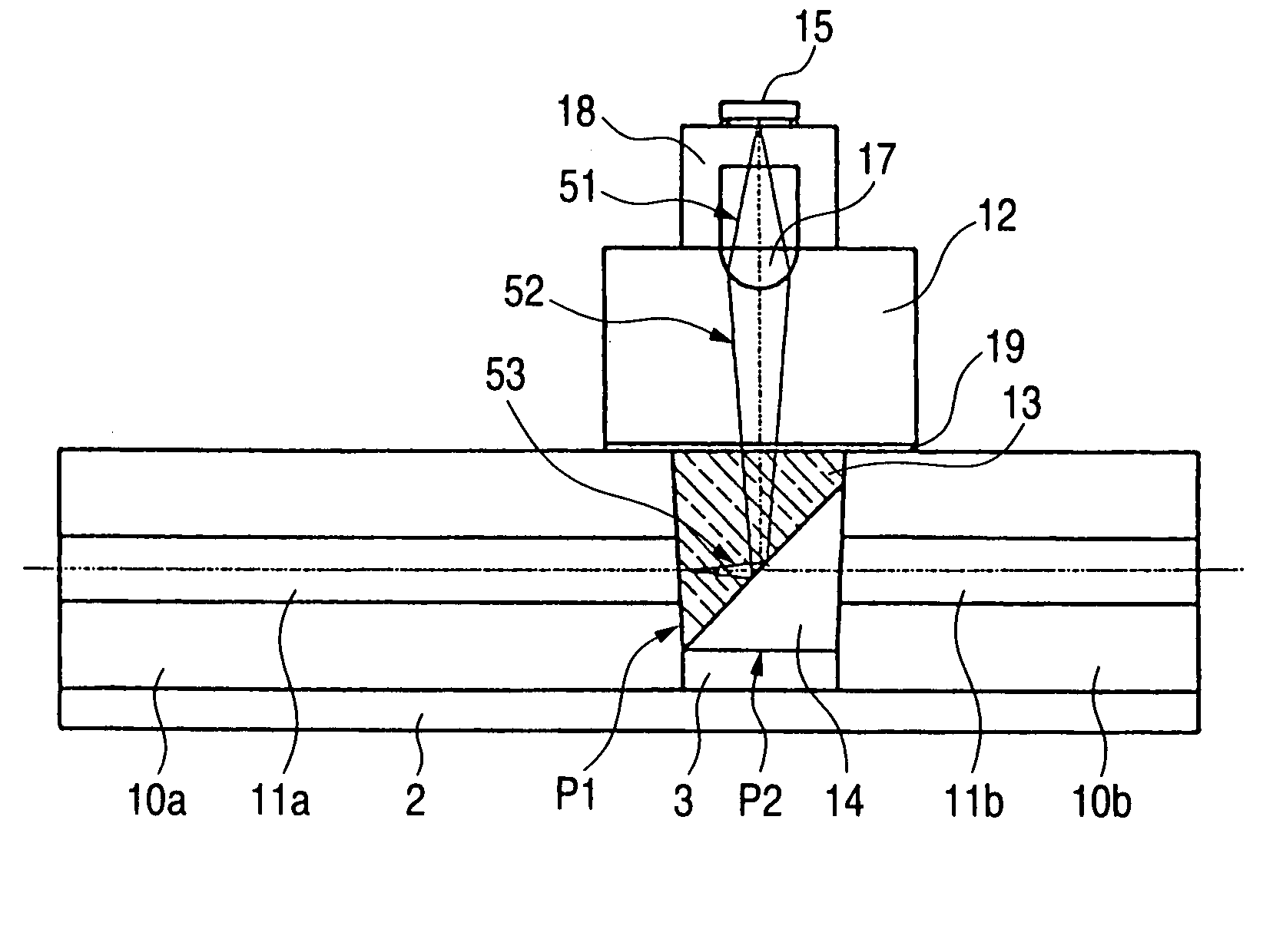
[0029]FIGS. 1A and 1B are views typically showing a first embodiment of an optical connection device according to the invention. A subject of this embodiment is an optical connection device for optically coupling light beams emitted from light-emitting elements such as a surface emission laser array 15 to an optical waveguide array 11a through a light-condensing unit such as a microlens array 17. FIG. 1A is a sectional view taken in a direction perpendicular to optical axes of the optical waveguides. FIG. 1B is a sectional view taken in a direction parallel to the optical axes.

[0030]As shown in FIG. 1A, the surface emission laser array 15 has a plurality of surface emission laser devices arranged in a row on a substrate at regular intervals of a pitch equal to the pitch of arrangement of optical waveguides in the optical waveguide array which will be described later. Although four devices are shown in FIG. 1A, the number of devices is not limited. Even a single device ...

embodiment 2

[Embodiment 2]

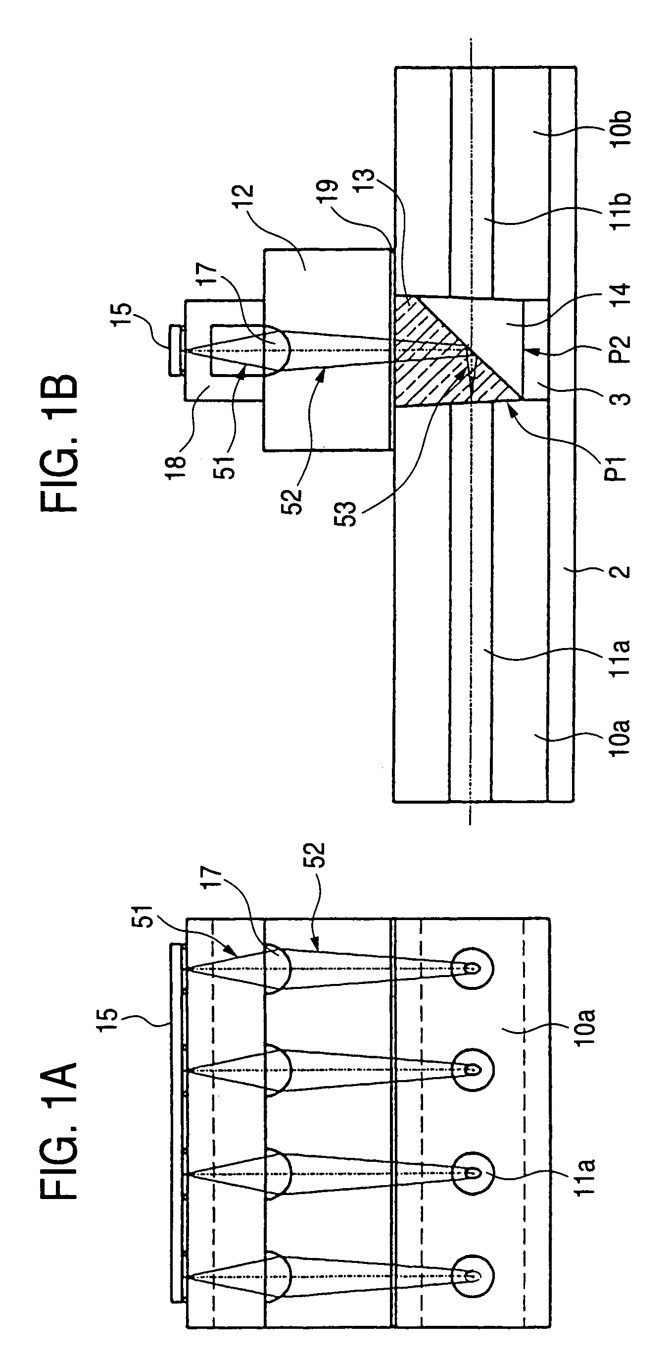
[0051]A second embodiment of the optical connection device according to the invention is functionally identical to Embodiment 1. In Embodiment 1, an optical waveguide array having a turning optical unit was integrated with a light source unit or with a photo detector unit, and the two units were brought into a facing contact with each other on a plane for adjustment to thereby be aligned with each other. This embodiment differs from Embodiment 1 in that the light source unit or photo detector unit and the turning optical unit are aligned and integrated into one body in advance, and after that the integrated body is fitted and fixed into the optical waveguides for connection.

[0052]Referring to FIG. 2, this embodiment will be described below. FIG. 2 is a sectional view taken in a direction parallel to the optical axes of the optical waveguides.

[0053]A microprism 23 is first stuck to a surface of a microlens array substrate 22 where a microlens array 27 is formed. A subst...

embodiment 3

[Embodiment 3]

[0060]FIGS. 3A and 3B are views typically showing a third embodiment of the optical connection device according to the invention. The function of the optical connection device according to this embodiment is as follows. A plurality of optical signals input from an optical waveguide array 31a are received by a plurality of photodetecting elements such as a photodiode array 36 and converted into electronic signals respectively. On the other hand, light beams emitted from a plurality of light sources such as a surface emission laser array 35 are coupled to an optical waveguide array 31b. The optical connection device according to this embodiment integrally formed from these arrays 31a, 31b, 35 and 36. FIG. 3A is a top view of the optical connection device. FIG. 3B is a sectional view of the optical connection device taken in a direction parallel to optical axes.

[0061]This embodiment is the same as in Embodiment 1 or 2 in that the micro-slit 34 is formed in an opto-electro...


PUM


Abstract

An optical connection device according to the invention is an optical connection device for optically coupling light propagated through an optical waveguide to an optical element arranged outside the optical waveguide and with the following configuration. Part of the optical waveguide is removed so as to be shaped like a groove. The optical waveguide and the optical element are arranged so that an optical axis of the optical waveguide intersects an optical axis of the optical element at a specified angle inside the groove. An optical unit is arranged at a position of intersection of the optical axes for turning light by reflection from one optical axis along the other optical axis.

Description

[0001]The present application is based on Japanese Patent Application No. 2002-247129, the entire contents of which are incorporated herein by reference.BACKGROUND OF THE INVENTION[0002]1. Field of the Invention[0003]The present invention relates to an optical connection device used in the field of optical communications and particularly relates to an optical connection device which can be integrated for optically coupling light beams propagated through optical waveguides to optical elements respectively.[0004]2. Related Art[0005]The quantity of information processed by an information processor such as a computer has been increasing steadily. In conjunction with this tendency, the number of wiring circuits inside or between electronic circuit boards used for forming the information processor has increased, and higher-density mounting of electronic circuits is required. However, problems such as interference of signals between wiring circuits and propagation delay caused by increase ...

Claims


Application Information

Patent Timeline
IPC IPC(8): G02B6/26G02B6/12G02B6/122G02B6/42H01L31/0232H01S5/022
CPCG02B6/12004G02B6/122G02B6/42G02B2006/12104G02B6/4214G02B6/4246
Inventor NAKAMA, KENICHISEKIGUCHI, YUKINARIMIKAMI, OSAMUMURATA, YOSHIKAZUMIYAZATO, KENTAROU
Owner NIPPON SHEET GLASS CO LTD
Why Eureka
Try Eureka