Thin film magnetic memory device having data read current tuning function

a magnetic memory device and tuning function technology, applied in the direction of static storage, digital storage, instruments, etc., can solve the problems of disadvantageously deteriorating the operation reliability of the entire mram device, unable to effectively carry out the tunneling film screening in an acceleration test conducted using a high electric field, etc., to achieve the effect of efficient execution of a defect acceleration test and improving the reliability of the mram devi

Inactive Publication Date: 2006-01-24
RENESAS ELECTRONICS CORP
View PDF11 Cites 7 Cited by
  • Summary
  • Abstract
  • Description
  • Claims
  • Application Information

AI Technical Summary

Benefits of technology

[0031]It is another object of the present invention to provide a configuration of a thin film magnetic memory device capable of efficiently executing a defect acceleration test for clarifying the potential defect of a tunneling film which forms a magnetic tunnel junction.
[0033]The above-mentioned thin film magnetic memory device can adjust the quantity of the current passing through the magnetic storage portion (tunneling magneto-resistance element) during data read according to an external input. It is, therefore, possible to secure a sufficient data read margin even if the manufacturing irregularity of the magnetic storage portions exists.
[0035]The above-mentioned thin film magnetic memory device can set the quantity of the passing current of the magnetic storage portion in another operation mode corresponding to the burn-in test, to be larger than that in the normal operation mode. It is, therefore, possible to efficiently execute a defect acceleration test to improve the reliability of the MRAM device.

Problems solved by technology

In other words, even if the same bias voltage is applied, sense current Is carried to tunneling magneto-resistance element TMR largely changes depending on the manufacturing irregularity of the tunneling film thickness, so that the electric resistance value of tunneling magneto-resistance element TMR, i.e., the level of stored data cannot be accurately sensed from the voltage of the bit line.
In other words, if a thin tunneling film is manufactured due to manufacturing irregularity, there is a probability that an excessive tunnel current flows during an ordinary operation to disadvantageously deteriorate the operation reliability of the entire MRAM device.
Furthermore, while it is necessary to conduct a defect acceleration test to ensure the reliability of the tunneling film so as to evaluate the reliability of tunneling magneto-resistance element TMR, tunneling film screening cannot be effectively carried out in an acceleration test conducted applying a high electric field as executed for a conventional MOS (Metal Oxide Semiconductor) type LSI (Large Scale Integrated Circuit).

Method used


Image

  • Thin film magnetic memory device having data read current tuning function
  • Thin film magnetic memory device having data read current tuning function
  • Thin film magnetic memory device having data read current tuning function

Examples


first embodiment

(Modification of First Embodiment)

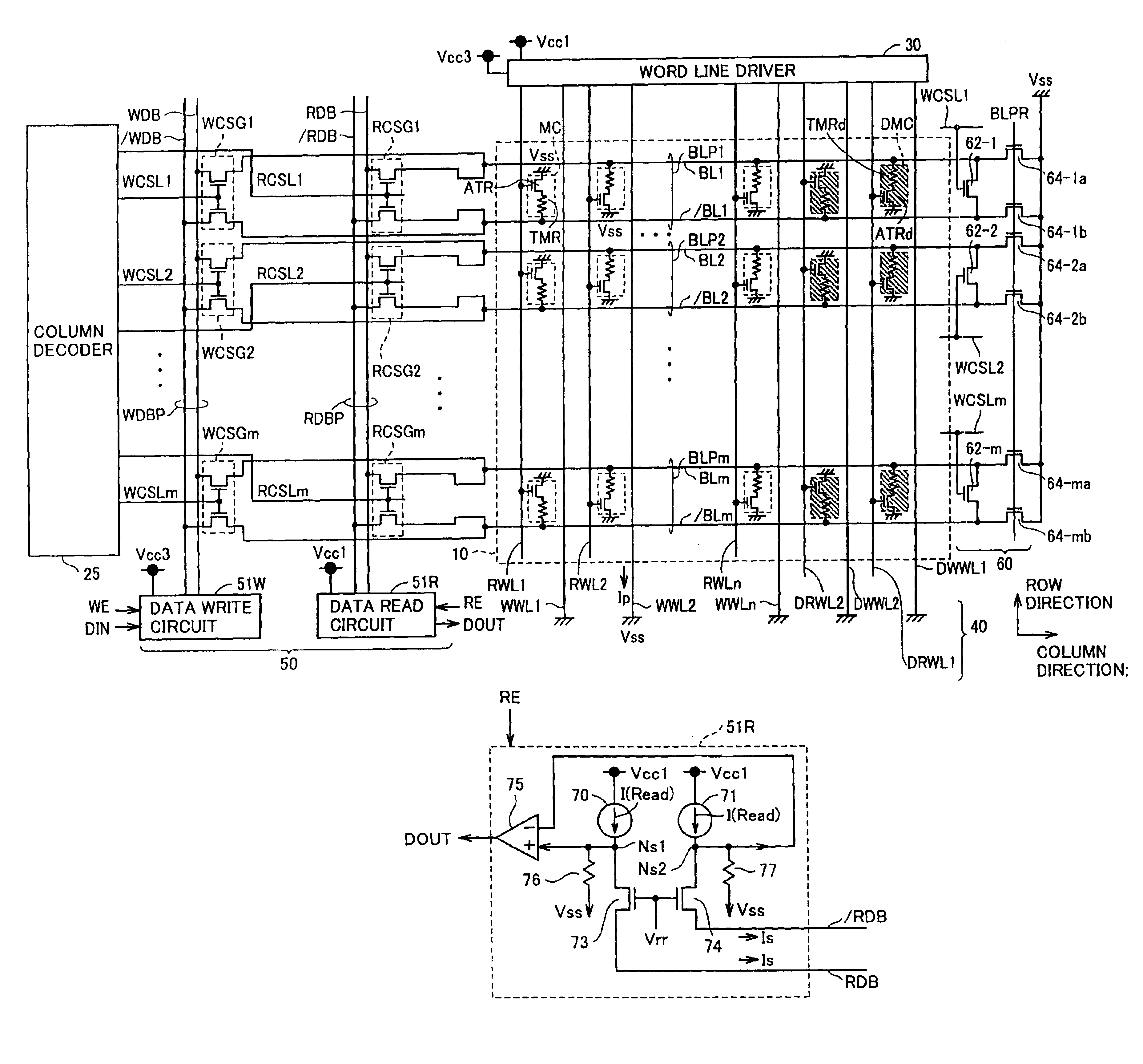
[0147]In a modification of the first embodiment, the configuration of MRAM device 1 in which sense current Is can be monitored during adjustment will be described.

[0148]Referring to FIG. 7, the configuration of constant current supply circuit 70 (71) included in data read circuit 51R in the modification of the first embodiment differs from the configuration thereof described in the first embodiment in that a current monitor section 190 which monitors the quantity of a current flowing in an internal node Ns1 (Ns2) is provided besides the constituent elements shown in FIG. 4. Since the other constituent elements of constant current supply circuits 70 and 71 are the same as those shown in FIG. 4, they will not be described herein repeatedly. In addition, since the constituent elements of data read circuit 51R other than constant current supply circuits 70 and 71 are the same as those shown in FIG. 3, they will not be described herein repeatedly.

[0149]C...

second embodiment

(Fourth Modification of Second Embodiment)

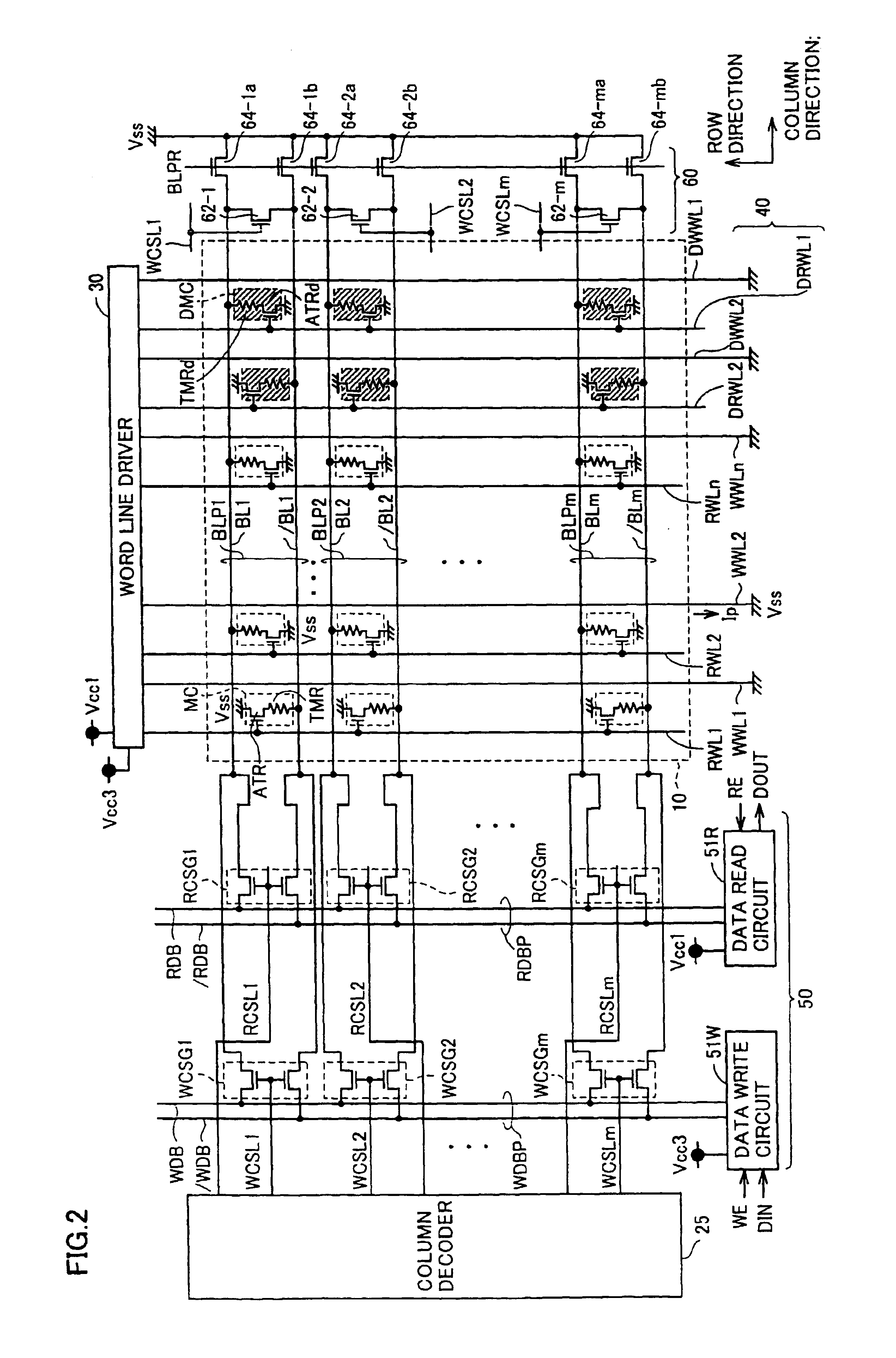
[0235]In memory array configuration in which a dummy memory cell is arranged on memory array 10 for comparison with a selected memory cell, one dummy memory cell is arranged for a plurality of MTJ memory cells. According to the memory array configurations shown in FIGS. 2 and 13, for example, two dummy memory cells are arranged for each memory cell column and one dummy memory cell is, therefore, arranged for each of the (n / 2) MTJ memory cell columns.

[0236]Due to this, compared with the access frequency of a normal MTJ memory cell, that of the dummy memory cell is high. In the burn-in test, therefore, it is possible to execute stricter screening to the dummy memory cells. In other words, in the burn-in test, it is necessary to apply a higher current stress to each dummy memory cell than that applied to each MTJ memory cell to thereby appropriately clarify the potential defect of the dummy memory cell.

[0237]In the fourth modification of the se...


PUM


Abstract

A constant current supply circuit generates a constant current according to a control voltage. A data read current passing through a tunneling magneto-resistance element constituting a memory cell during data write is set according to the constant current. Constant current supply circuit includes a voltage adjustment circuit generating a reference voltage adjustable according to an external input, a current source generating the constant current according to the reference voltage, and a voltage switch circuit transmitting the reference voltage to the current source as a control voltage during a normal operation.

Description

[0001]This application is a divisional of application Ser. No. 10 / 135,459 filed May 1, 2002, now U.S. Pat. No. 6,646,911, issued on Nov. 11, 2003.BACKGROUND OF THE INVENTION[0002]1. Field of the Invention[0003]The present invention relates to a thin film magnetic memory device, and more particularly relates to a random access memory provided with memory cells having magnetic tunnel junctions (MTJs).[0004]2. Description of the Background Art[0005]As a memory device capable of storing nonvolatile data with low consumption power, attention has been paid to an MRAM (Magnetic Random Access Memory) device. The MRAM device is a memory device which stores nonvolatile data using a plurality of thin film magnetic elements formed on a semiconductor integrated circuit and which can access each of the thin film magnetic elements.[0006]Recently, it has been made public that the performance of the MRAM device surprisingly advances by using tunneling magneto-resistance element which are thin film m...

Claims


Application Information

Patent Timeline
Patent Type & Authority Patents(United States)
IPC IPC(8): G11C16/04G11C11/15
CPCG11C11/15G11C11/1673G11C29/028G11C11/1675G11C11/1655G11C29/04G11C29/06G11C29/021G11C2029/0403G11C2029/0409G11C29/48
Inventor HIDAKA, HIDETO
Owner RENESAS ELECTRONICS CORP
Why Eureka
Try Eureka