Dielectric separation type semiconductor device and method of manufacturing the same
- Summary
- Abstract
- Description
- Claims
- Application Information
AI Technical Summary
Benefits of technology
Problems solved by technology
Method used
Image

Examples
embodiment 1
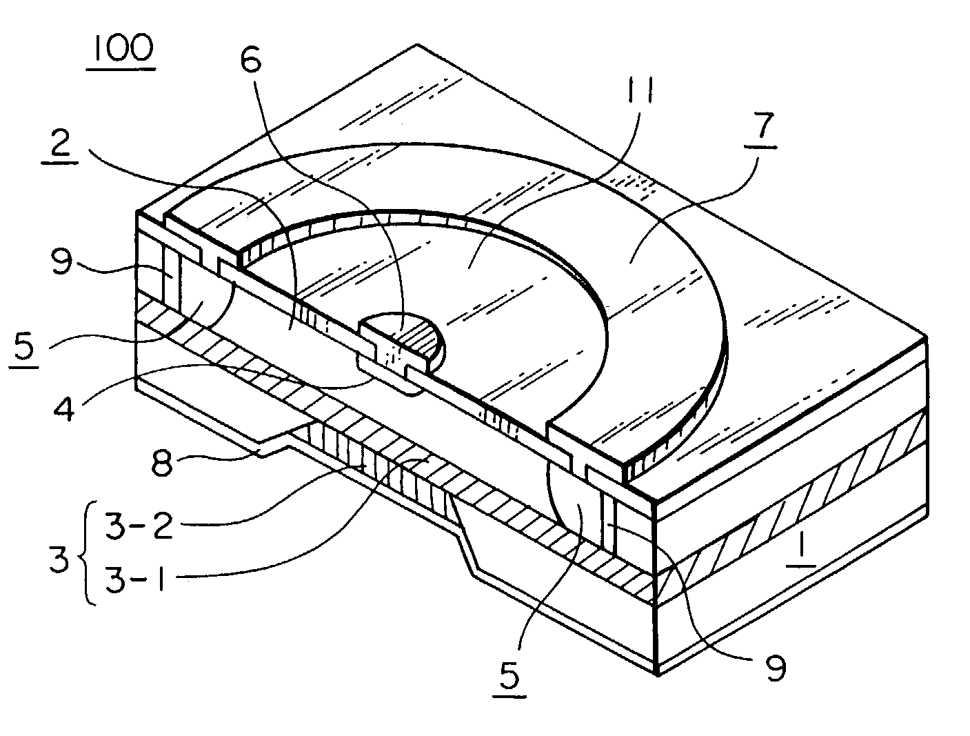
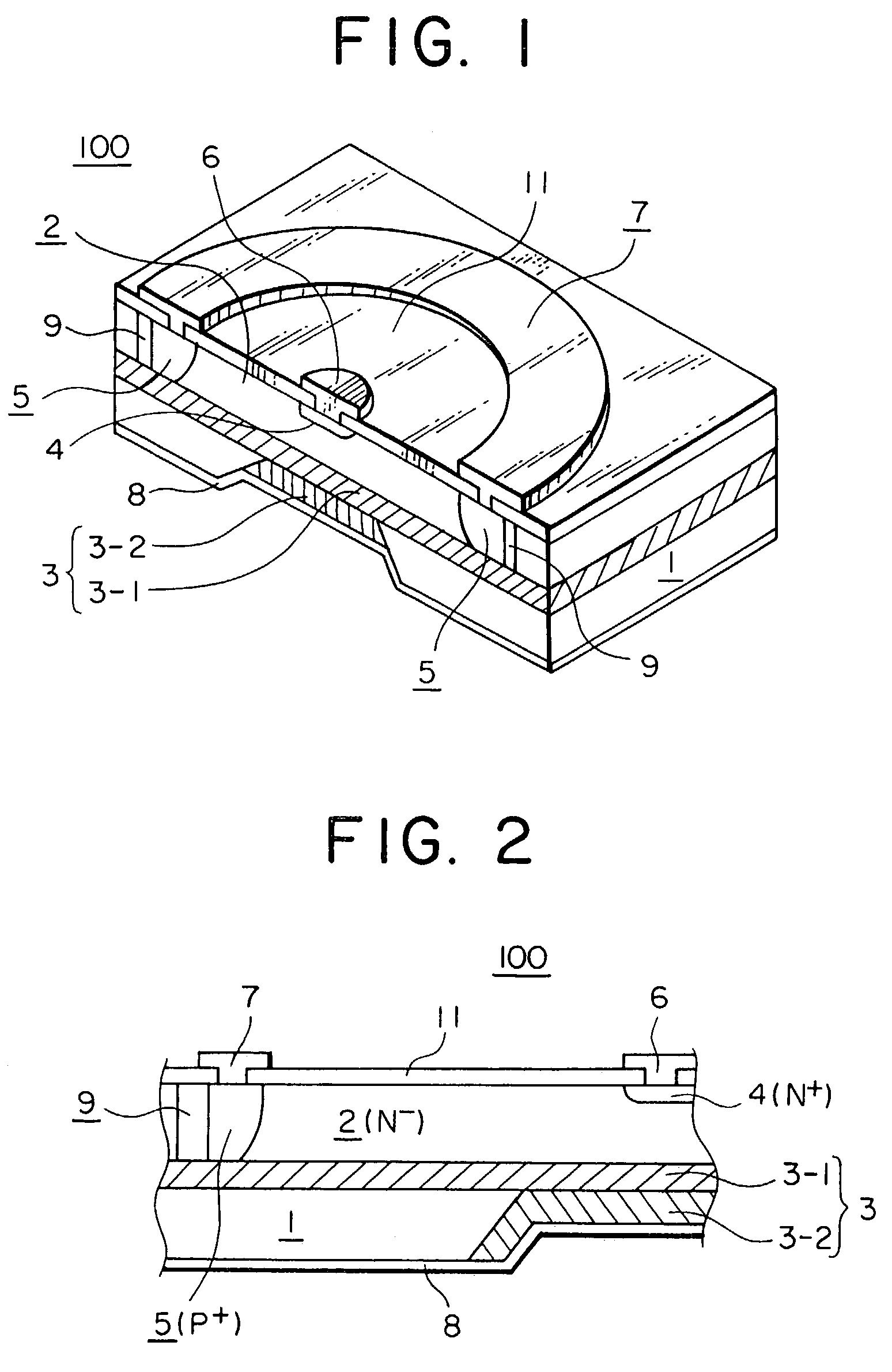
[0063]Now, a first embodiment of the present invention will be described by reference to the drawing. FIG. 1 is a perspective view showing partially in section a dielectric separation type semiconductor device 100 according to the first embodiment of the present invention, and FIG. 2 is a sectional view showing a portion of the semiconductor device 100 shown in FIG. 1.
[0064]Referring to FIGS. 1 and 2, the dielectric separation type semiconductor device 100 is comprised of a semiconductor substrate 1, an n−-type semiconductor layer 2, a dielectric layer generally denoted by reference numeral 3, an n+-type semiconductor region 4, a p+-type semiconductor region 5, electrodes 6 and 7, a evaporated back-surface electrode (hereinafter referred to simply as “back-surface electrode”) 8 and insulation films 9 and 11.
[0065]The dielectric layer 3 and the back-surface electrode 8 are formed, respectively, on the top and bottom or back surfaces of the semiconductor substrate 1.
[0066]The n−-type ...
embodiment 2
[0119]In conjunction with the first embodiment of the present invention, no consideration has been paid to the process of forming the semiconductor device 100 shown in FIG. 7. A second embodiment of the present invention is directed to a method of manufacturing the semiconductor device 100 by forming the dielectric layers 3-1, respectively, on both surfaces of the active layer substrate, implanting nitrogen into the major surface of the active layer substrate, bonding the semiconductor substrate 1 composed of a pedestal silicon and forming an electrode pattern.
[0120]In the following, description will be made of a method of manufacturing the dielectric separation type semiconductor device 100 by bonding the pedestal silicon substrate onto the active layer substrate after the nitrogen implantation according to the second embodiment of the invention by reference to FIGS. 11 to 13 which illustrates in sectional views the processes or steps involved in this method.
[0121]Incidentally, in ...
embodiment 3
[0132]In the method of manufacturing the dielectric separation type semiconductor device according to the second embodiment of the invention, the semiconductor substrate 1 is bonded to the active layer substrate 21 after the nitrogen implantation. A third embodiment of the invention is directed to a method of manufacturing the dielectric separation type semiconductor device 100 by bonding the active layer substrate 21 onto the semiconductor substrate 1 after having formed a dielectric layer on the semiconductor substrate by a thermally nitrided film or a CVD nitride film.
[0133]In the following, referring to FIGS. 14 to 16, description will be made of the method of manufacturing the dielectric separation type semiconductor device 100 by bonding the active layer substrate 21 onto the semiconductor substrate 1 after having formed on the semiconductor substrate 1 a thermally nitrided film or a CVD nitride film (dielectric layer) according to the third embodiment of the present invention...
PUM
 Abstract
Description
Claims
Application Information
 - Generate Ideas
- Intellectual Property
- Life Sciences
- Materials
- Tech Scout
- Unparalleled Data Quality
- Higher Quality Content
- 60% Fewer Hallucinations
Browse by: Latest US Patents, China's latest patents, Technical Efficacy Thesaurus, Application Domain, Technology Topic, Popular Technical Reports.
© 2025 PatSnap. All rights reserved.Legal|Privacy policy|Modern Slavery Act Transparency Statement|Sitemap|About US| Contact US: help@patsnap.com