Scanning exposure apparatus

a technology of exposure apparatus and scanning lens, which is applied in the direction of photomechanical apparatus, instruments, printers, etc., can solve the problems of requiring a considerable amount of labor and considerable time to analyze and check, and achieve the effect of quick analysis of a caus

Inactive Publication Date: 2006-01-31
NIKON CORP
View PDF12 Cites 175 Cited by
  • Summary
  • Abstract
  • Description
  • Claims
  • Application Information

AI Technical Summary

Benefits of technology

[0006]Accordingly, it is an object of the present invention to provide a scanning exp

Problems solved by technology

When the exposure line widths of patterns formed on the individual shot areas of the substrate vary, the conventional scanning exposure apparatus cannot quickly f

Method used


Image

  • Scanning exposure apparatus
  • Scanning exposure apparatus
  • Scanning exposure apparatus

Examples


second embodiment

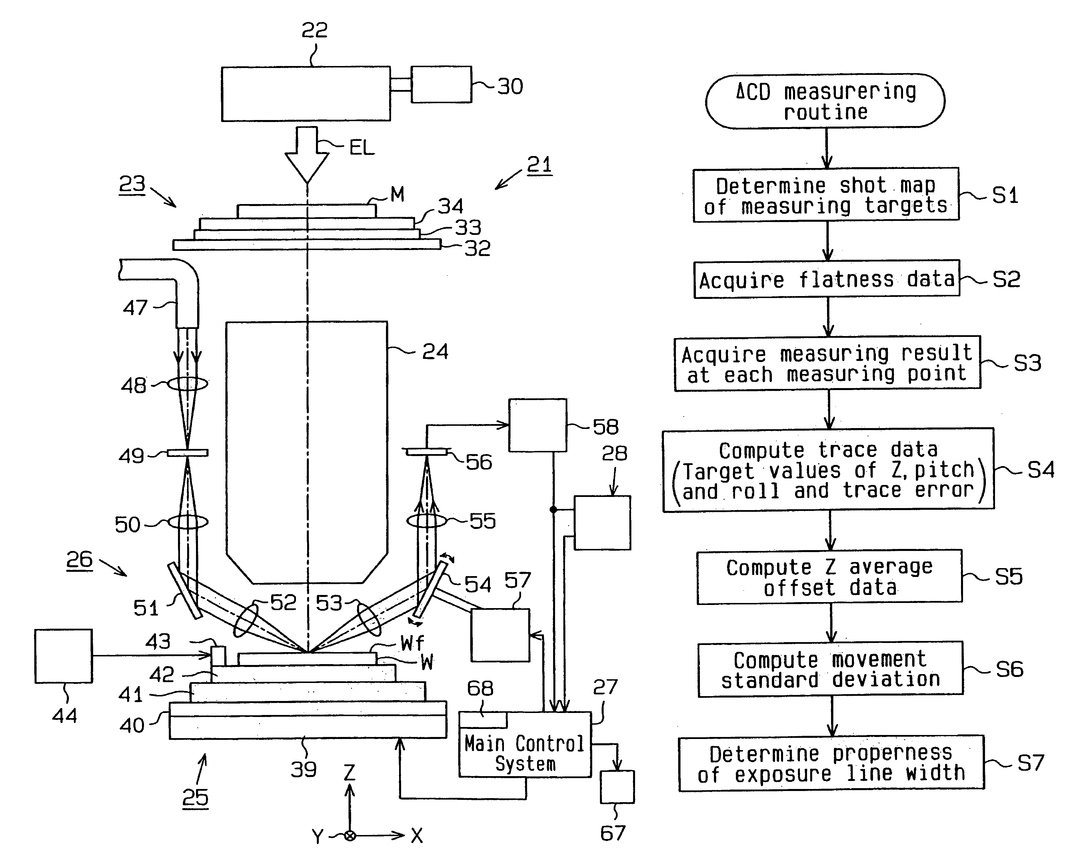
[0180]A second embodiment of the scanning exposure apparatus according to the present invention will now be described referring to FIGS. 22 and 23.

[0181]In the first embodiment, the ΔCD management apparatus 28 is provided as separate from the main control system 27 of the scanning exposure apparatus 21. In the second embodiment, a ΔCD management apparatus 28A having the equivalent capabilities of the ΔCD management apparatus 28 is incorporated in the main control system 27. The ΔCD management apparatus 28A differs from the ΔCD management apparatus 28 only in that it does not have the input section 93 and the display section 94. In the second embodiment, data such as the measured line width can be input through an unillustrated input device provided in the scanning exposure apparatus 21. Data of various graphs generated by the ΔCD management apparatus 28A is stored in a memory 68 as a data storage section in the main control system 27. Therefore, a display device 67 can display graph...

third embodiment

[0184]A third embodiment of the scanning exposure apparatus according to the present invention will now be discussed.

[0185]In the third embodiment, the CPU 90 as image-state prediction means has an image-forming simulation capability (image-forming simulation means) added to the CPU of the first embodiment to calculate the exposure line width as the state of the image of a pattern or the variation amount of the exposure line width. The CPU 90 of the third embodiment does not therefore require storage of the data shown in FIG. 18. The third embodiment is the same as the first embodiment in other points.

[0186]The image-forming simulation capability is to compute the exposure line width or the variation amount of the exposure line width based on data of the Z average offset and movement standard deviation in addition to various performances of the projection optical system 24, such as the designed line width of a pattern, the defocus amount (the amount of the Z-directional deviation of...


PUM


Abstract

A scanning exposure apparatus which promptly analyzes a cause for a variation in exposure line width. The scanning exposure apparatus includes a mask stage on which a mask is placed, a wafer stage on which a wafer is placed, a focusing mechanism which detects surface position information of the wafer and adjustment means which adjusts the surface position of the wafer. Control means acquires pose information of the wafer adjusted by the adjustment means at the time of exposure and stores the pose information in a memory in association with preacquired surface shape information of an exposure area. A state in which the exposed surface of the wafer has been exposed with respect to exposure light is known from the pose information and the surface shape information.

Description

CROSS-REFERENCE TO RELATED APPLICATIONS[0001]This application is a divisional application of U.S. patent application Ser. No. 10 / 085,211, filed Feb. 27, 2002 now U.S. Pat. No. 6,538,721, which is a continuation-in-part application of U.S. patent application Ser. No. 09 / 817,316 filed on Mar. 26, 2001 now abandoned, entitled “Scanning Exposure Apparatus”.BACKGROUND OF THE INVENTION[0002]The present invention relates to a scanning exposure apparatus, and, more particularly, to a scanning exposure apparatus which is used in the lithography process for fabricating micro devices, such as a semiconductor device, liquid crystal display device, image pickup device (CCD or the like) and thin-film magnetic head.[0003]One known scanning exposure apparatus of this type comprises a mask stage on which a photomask or reticle (hereinafter called “mask”) having a circuit pattern formed thereon is to be placed, a substrate stage on which a substrate (wafer, glass plate or the like) coated with a phot...

Claims


Application Information

Patent Timeline
IPC IPC(8): G03B27/42G03F7/20G03F9/00
CPCG03F7/70358G03F9/7026G03F9/7011G03F7/70691
Inventor OKITA, SHINICHIHAGIWARA, TSUNEYUKI
Owner NIKON CORP
Why Eureka
Try Eureka