Electrostatically operated micro-optical devices and method for manufacturing thereof

a micro-optical device and optical technology, applied in the field of electro-optical-operated micro-optical devices, can solve the problems of unbalanced force of both sides of finger electrodes, etc., and achieve the effects of reducing the displacement, improving the optical performance, and reducing the force outpu

Inactive Publication Date: 2006-02-07
ASIA PACIFIC MICROSYST
View PDF8 Cites 59 Cited by
  • Summary
  • Abstract
  • Description
  • Claims
  • Application Information

AI Technical Summary

Benefits of technology

[0008]The present invention has been made in view of the above micro-optical device function requirements, and it is an object of present invention to provide micro-optical devices using an electrostatic microactuator having new spring designs to overcome side instability and exhibit enlarged displacement, and to provide micro-optical devices using an electrostatic microactuator having new designs of comb finger electrode shapes to generate larger force output, and to provide a new optical light path design in conjunction with said electrostatic microactuator to render the made micro-optical devices exhibiting better optical performance, and to provide micro-optical devices using an electrostatic comb drive actuator having new latch mechanism to maintain the micro-optical device at particular state without additional electrical load on the electrostatic microactuator, and to provide process techniques to manufacture the micro-optical devices with said electrostatic microactuator in a mass production manner with higher yield.
[0013]In accordance with other aspect of the present invention, an off-axis light path layout design enabling less coupled back-return-loss for said micro-optical devices is invented for analogically controlling the light attenuation.
[0014]In accordance with other aspect of the present invention, a clip type latch using friction force or electrostatic force mechanism is invented for said micro-optical devices to maintain the status of said micro-optical devices at certain condition without power consumption.
[0015]According to the present invention, many ways can be provided to make the mirror surface smoothness of said micro-optical devices in a mass production manner with higher production yield, including but not limited to applying the silicon etching solution to reduce the surface roughness; adopting the (110) oriented silicon substrate in conjunction with post-etching in the silicon etching solution; and oxidizing the mirror surface after the mirror side wall is formed.
[0016]According to the present invention, many ways can be provided to make the packaging process of said micro-optical devices in a mass production manner with higher production yield, including but not limited to lid capping on the substrate to protect the fragile MEMS elements; making flow channels and trenches on the substrate to avoid the movable and suspended MEMS elements being attacked by the sealing and assembling materials like glues, epoxy, solders, etc; and dicing the devices form substrates, then became discrete dies when the MEMS elements have been protected by lids.

Problems solved by technology

However, it will also lead to a requirement that the corresponding MEMS actuator has to be able to provide enough displacement to let micromirror fully block or reflect the incoming light beam.
The tiny deviations of comb finger and gap width will cause the unbalanced force of both sides of finger electrode, and such deviation is easily induced by microfabrication process.
The unbalanced force of both sides of finger electrode is the major contribution factor to the side sticking effect.

Method used


Image

  • Electrostatically operated micro-optical devices and method for manufacturing thereof
  • Electrostatically operated micro-optical devices and method for manufacturing thereof
  • Electrostatically operated micro-optical devices and method for manufacturing thereof

Examples


first embodiment

The First Embodiment

[0034]Again, due to the side instability issue, and requirement of longer traveling distance of micro-mirror 214, i.e., the displacement of comb drive actuator, we proposed a micro-optical device 310 using electrostatic comb drive actuators having thinned spring structure 312 as shown in FIG. 3. Let us go through the fundamental physics with respect to the mechanics of comb drive actuator. FIG. 3 shows the well-adopted comb drive actuator design with folded-beam spring 311. Such design has been reported to show increased displacement under the same actuation voltage comparing with traditional spring design, since the spring constant in and perpendicular to moving direction can become smaller and larger, respectively. (See for example, V. P. Jaecklin, C. Linder, N. F. de Rooij, and J. M. Moret, “Micromechanical Comb Actuators with Low Driving Voltage,” J. Micromech. Microeng., Vol. 2, 1992, pp. 250–255; R. Legtenberg, A. W. Groeneveld, and M. Elwenspoek, “Comb-dri...

second embodiment

The Second Embodiment

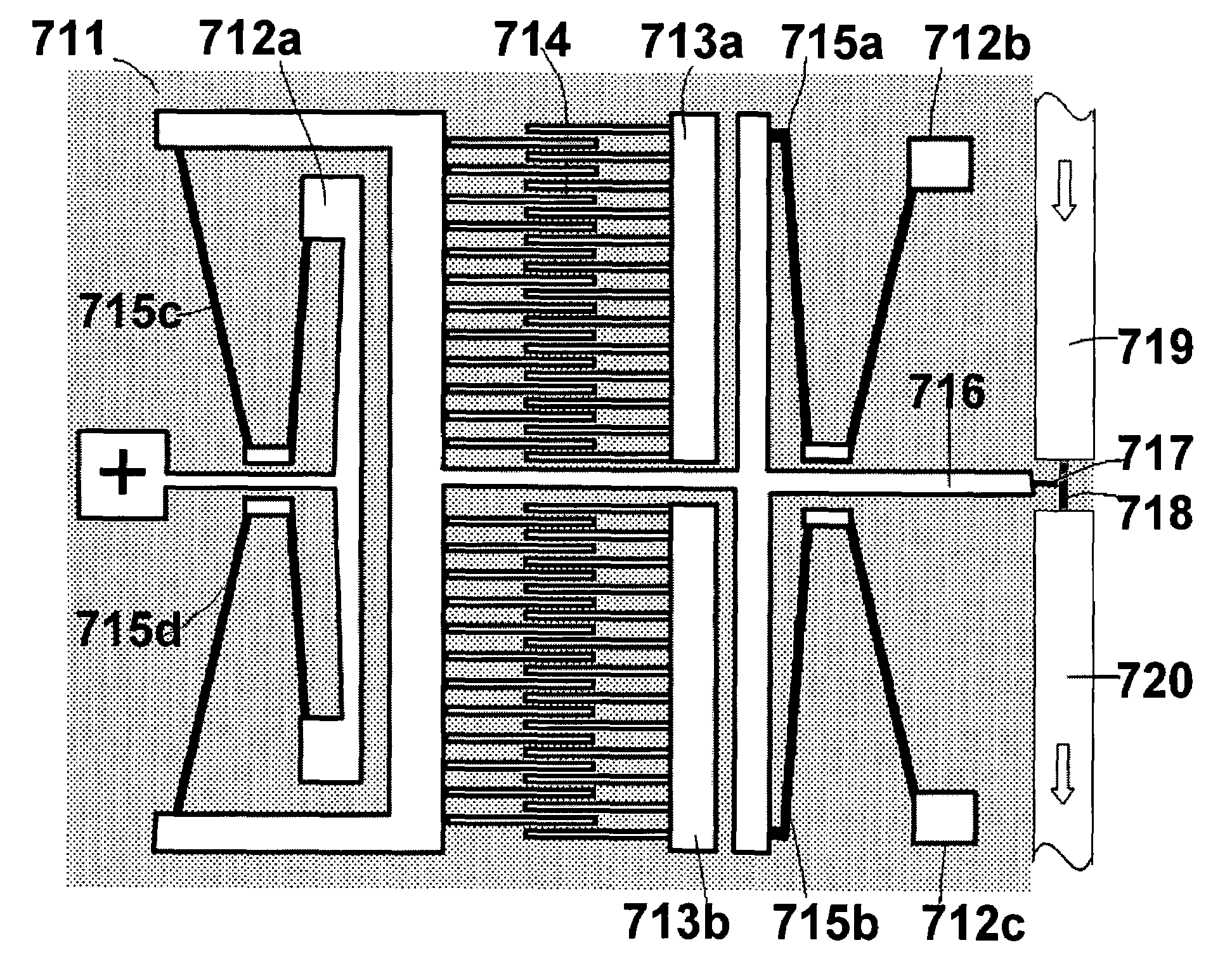
[0038]According to another aspect of our invention, the micro-optical devices 100 shown in FIG. 1 or micro-optical devices 310 shown in FIG. 3 can be modified into the layout configuration shown in FIG. 6. To further reduce the instability influence from the moment contributed by the lateral electrostatic force of comb electrodes, all the spring anchors are assigned symmetrically at both sides of comb electrodes. By using such symmetric layout in conjunction with our spring thinning approach, we are able to make the comb drive actuator exhibit enlarged displacement and robustness to instability.

[0039]The micro-optical device 611 that is disclosed in the present invention as shown in FIG. 6 comprises a reflective mirror 617 on one side of a shuttle beam 616, a set of suspended springs 615a, 615b which supports the shuttle beam 616 at their free ends and fixed onto a substrate via anchors 612b, 612c, a set of movable comb drive electrodes 614 that is connected wit...

third embodiment

The Third Embodiment

[0051]In according to the other aspect of our invention, we proposed micro-optical devices using comb drive actuator 1050 based on a stationary comb finger electrode of a shape with oblique angle 1051, and a movable comb finger electrode of a shape with oblique angle 1052, as shown in FIG. 10b. Thereby the force output from said comb drive actuator is enlarged based on this approach. Basically the generated electrostatic force from the comb drive actuator is contributed by the electrostatic field between the two comb finger electrodes.

[0052]The displacement of the movable comb finger electrode 1052 from its original rest position is a result of force balance between the electrostatic force and spring restoration forces along with the travel direction and perpendicular direction of travel direction. i.e., denoted as spring force 1004 and spring force 1003. The spring design mentioned in present embodiment is one of our inventions disclosed in embodiments 1 and 2.

[...


PUM


Abstract

Electrostatically operated micro-optical devices and method of manufacturing such devices is disclosed. In a preferred embodiment, the micro-optical devices using electrostatic comb drive actuators having new spring designs to overcome side instability and exhibit enlarged displacement, having new designs of comb finger electrode shapes to generate larger force output, and having new clip type latch mechanism to control the corresponding device at certain states in an analog manner without electrical power consumption. Based on the proposed optical path and device configurations, integration and assembly of a plurality of reflective micro-mirrors in conjunction with proposed new comb drive actuators is very promising way to provide micro-optical devices to get good optical performance and suitable for multi-channel applications. We also disclose several process techniques to manufacture the micro-optical devices with said electrostatic comb drive actuator in a mass production manner with higher yield.

Description

BACKGROUND OF THE INVENTION[0001]1. Field of the Invention[0002]This invention is related to electrostatically operated micro-optical devices and method of manufacturing such devices.[0003]2. Description of the Prior Art[0004]Considerable interest has recently been shown in optical microelectromechanical systems (optical MEMS) based on comb drives using an electrostatic actuation scheme. Combining the comb-drive actuator with the silicon-on-insulator (SOI) and deep-reactive-ion-etching (DRIE) process, many MEMS based components have been demonstrated such as optical switch, variable optical attenuator (VOA), and Fourier transform spectrometer (FTS), etc. It can be seen that, for example, W. Noell, et al., “Applications of SOI-Based Optical MEMS”, IEEE J. on Selected Topics in Quantum Electronics, Vol. 8, No. 1, January / February 2002, pp. 148–154; C. Marxer, et al., “A Variable Optical Attenuator Based on Silicon Micromechanics”, IEEE Photonics Technol. Lett., Vol. 11, No. 2, 1999, p...

Claims


Application Information

Patent Timeline
Patent Type & Authority Patents(United States)
IPC IPC(8): G02B6/26G02B6/35
CPCG02B6/358G02B6/357G02B6/3514G02B6/3546G02B6/3552G02B6/3594G02B6/3584
Inventor CHEN, CHIH-CHUNGLEE, CHENGKUOLAI, YEN-JYHCHEN, WEN-CHIHTSAI, MING-HUNG
Owner ASIA PACIFIC MICROSYST
Why Eureka
Try Eureka