Nonvolatile semiconductor memory device and method for providing security for the same

a technology of nonvolatile semiconductors and memory devices, applied in the direction of unauthorized memory use protection, instruments, computing, etc., can solve the problems of increasing the circuit size of a memory chip, affecting the security of classified information, and more conspicuous, so as to achieve the effect of further enhancing the function of providing security and enhancing the security

Inactive Publication Date: 2006-02-07
PANASONIC CORP
View PDF10 Cites 80 Cited by
  • Summary
  • Abstract
  • Description
  • Claims
  • Application Information

AI Technical Summary

Benefits of technology

[0020]In this embodiment, the column latch circuit provided in advance in the nonvolatile semiconductor memory device and its function of performing a program verifying operation can be utilized to perform the operation of security authentication. Therefore, a security function is realized with a few additional circuits and without adopting an additional operational mode. As a result, it is possible to avoid an increase in the complexity of operation control and an increase in circuit size due to the addition of the security function.
[0021]The inventive memory device may start the latching operation and verifying operation when a security function deactivation command has been inputted or when at least a specified address or specified data has been inputted, and may further include a register for arbitrarily setting the security function deactivation command, specified address and specified data. In such an embodiment, the security function deactivation command, specified address and specified data can be arbitrarily set for each user or for each chip. Therefore, if a method for deactivating the security function is not open to the public, it is difficult for a malicious third party to identify the security function deactivation method. As a result, the function of providing security can be further enhanced.
[0022]When it is detected that the password is prohibited data, access to a memory cell array from outside is preferably prevented. In such an embodiment, it is possible to eliminate malicious access gained by using a password that is not identical to the security function deactivation code and deactivating the security function.
[0024]In still another embodiment, the security function is not deactivated if the specified address is not inputted before the operation of latching a password in the column latch circuit, or if at least the specified address or the specified data is not inputted before the verifying operation for determining whether the password is identical to the security function deactivation code stored in the deactivation code storing memory cells, and a register for arbitrarily setting the specified address and specified data is further provided. In such an embodiment, the specified address and the specified data can be arbitrarily set for each user or for each chip. Therefore, if the security function deactivation method is not open to the public, it is difficult for a malicious third party to identify the security function deactivation method. As a result, the function of providing security can be further enhanced.
[0025]The inventive memory device may further include: a data scrambling circuit for scrambling the password and for outputting the scrambled password to the column latch circuit; and a means for resetting data latched in the column latch circuit when it is determined that the password is not identical to the security function deactivation code during the verifying operation. In such an embodiment, the function of providing security can be further enhanced.

Problems solved by technology

If these programs or pieces of information can be illegally read out or freely rewritten by a third party, critical problems occur in terms of security for classified information.
First, as shown in FIG. 20, the conventional security circuit has to be additionally provided with: the password storage circuit; and the comparator for making a comparison between the password stored in the password storage circuit and the password inputted through the data terminal, thus increasing the circuit size of a memory chip. However, in accordance with the trend toward miniaturization of equipment, the nonvolatile semiconductor memory device also needs to be reduced in size since the increase in circuit size as mentioned above becomes a contributory factor to inhibiting the miniaturization of equipment. Further, as a conceivable measure to enhance the security function, the number of bits for password may be increased. However, if the number of bits is increased, the password storage circuit and the comparator further increase in size, thus making the above-described problem more conspicuous.
Secondly, in order to implement the security function in the nonvolatile semiconductor memory device, it is necessary to put the memory device into not only a conventional operational mode but also another operational mode, i.e., a security authentication mode in which the password stored in the password storage circuit is compared with the password inputted through the data terminal. To adopt another operational mode in this manner adversely increases the complexity and size of a control circuit.

Method used


Image

  • Nonvolatile semiconductor memory device and method for providing security for the same
  • Nonvolatile semiconductor memory device and method for providing security for the same
  • Nonvolatile semiconductor memory device and method for providing security for the same

Examples


first embodiment

[0048](First Embodiment)

[0049]Circuit Configuration

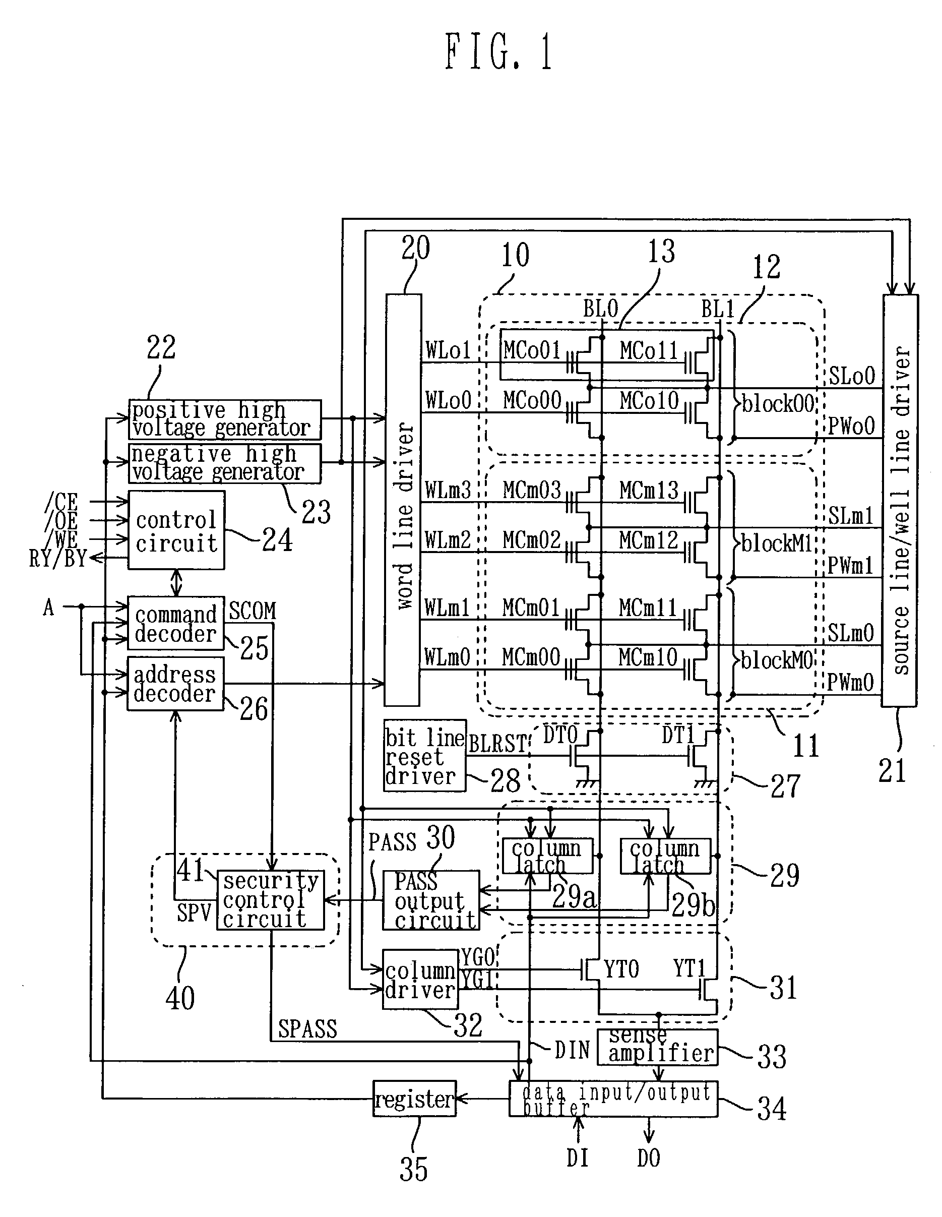
[0050]FIG. 1 is a circuit diagram showing the configuration of a nonvolatile semiconductor memory device (flash memory) according to a first embodiment. As shown in FIG. 1, the nonvolatile semiconductor memory device of the present embodiment includes: a memory cell array 10; and a peripheral circuit that operates when data is stored in the memory cell array 10 and when data is read out from the memory cell array 10.

[0051]The memory cell array 10 includes a plurality of memory cells MCm00 to MCm13 and memory cells MCo00 to MCo11 that are arranged in rows and columns. The memory cell array 10 is divided into a main region 11 that is open to a user and an optional region 12 that is not open to a user. In the main region 11, a plurality of memory cells MCm00 to MCm13 (normal memory cells) are arranged. On the other hand, in the optional region 12, a plurality of memory cells MCo00 to MCo11 are arranged, and a security function deactiva...

second embodiment

[0157](Second Embodiment)

[0158]In the verifying operation of the first embodiment, if all the latch data is data “1” at the start of the verifying operation, all the latch data after the verifying operation is data “1” irrespective of the data in the security function deactivation code stored in memory cells, and therefore, the PASS output circuit 30 is bound to output a high-level PASS signal as a result of the verifying operation. Accordingly, if a password in which all the data is “1” is stored in the column latch circuit 29, the security function can be deactivated irrespective of the data in the security function deactivation code. Therefore, a means for detecting that input latch data is prohibited data is provided in the second embodiment. As used herein, the prohibited data refers to, when all bits of input data are organized into a group or divided into two or more groups, input data having a group of bits in which all the data is “1”. In other words, the prohibited data re...

third embodiment

[0192](Third Embodiment)

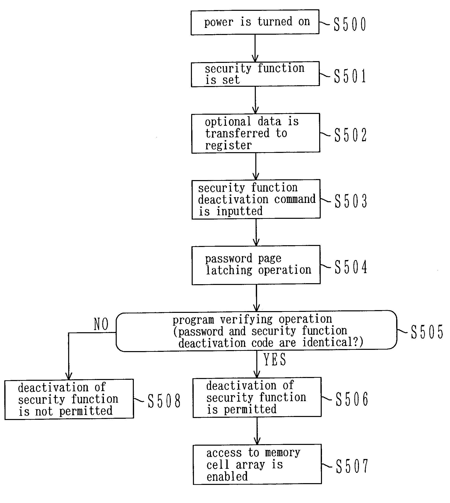
[0193]In the first and second embodiments, when the security function deactivation command is inputted, a password for deactivating the security function is inputted by performing the page latching operation, and then the verifying operation is performed to whether or not the password is identical to the security function deactivation code. And if the password and the security function deactivation code are identical, the security function is deactivated. The security is ensured in this manner in the first and second embodiments. In the first and second embodiments, each of the settings of the address terminal A during the page latching operation, the address terminal A during the verifying operation, and the data input terminal DI during the verifying operation is an arbitrary setting “Don't Care”.

[0194]In the third embodiment, the nonvolatile semiconductor memory device is provided with a means for detecting that a specified address is inputted before the p...


PUM


Abstract

An inventive nonvolatile semiconductor memory device is provided, in advance, with a column latch circuit 29 for performing a batch write operation (page latching operation, page programming operation, and verifying operation), and the column latch circuit 29 is utilized to realize a security function. The inventive memory device is further provided with a security control circuit 41 for carrying out control so that a password for deactivating the security function is stored in the column latch circuit 29 and a verifying operation is performed to determine whether the password stored in the column latch circuit 29 is identical to a security function deactivation code stored in a deactivation code storage 13. If it is determined that the password and the security function deactivation code are identical as a result of the verifying operation, the security function is deactivated.

Description

BACKGROUND OF THE INVENTION[0001]The present invention generally relates to nonvolatile semiconductor memory devices including security protection mechanisms and capable of electrically rewriting data, and methods for providing security for the devices.[0002]In recent years, nonvolatile semiconductor memory devices typified by flash memories have been used in various fields since they are not only capable of electrically rewriting data but also capable of retaining data even if the devices are turned off. For example, nonvolatile semiconductor memory devices are used as memory devices for storing data in systems such as cellular phones, digital cameras and silicon audio players. Nonvolatile semiconductor memory devices are also used as internal memory devices of microcomputers provided in, for example, IC cards.[0003]Nonvolatile semiconductor memory devices store therein, for example, programs for allowing systems to operate in accordance with desired procedures, information concern...

Claims


Application Information

Patent Timeline
Patent Type & Authority Patents(United States)
IPC IPC(8): G06F12/14G11C16/22
CPCG06F12/1433G11C16/22G06F12/1466
Inventor KOUNO, KAZUYUKI
Owner PANASONIC CORP
Why Eureka
Try Eureka