Structure and method for fabricating a bond pad structure

a technology of bonding pads and structures, applied in the direction of semiconductor/solid-state device manufacturing, electric devices, solid-state devices, etc., to achieve the effect of more support and large area

Active Publication Date: 2006-02-14
CHARTERED SEMICONDUCTOR MANUFACTURING
View PDF9 Cites 39 Cited by
  • Summary
  • Abstract
  • Description
  • Claims
  • Application Information

AI Technical Summary

Benefits of technology

[0015]The buffer pad and the (bond pad) support layer under the bond pad provide the stress relief needed so that the integrity of the dielectric layers is not destroyed during the bonding process. Furthermore, the buffer pad can have a larger area than the bond pad and therefore can provide more support.

Problems solved by technology

For instance, some of these advantages may be mutually contradictory, in that they cannot be simultaneously present in a single embodiment.

Method used


Image

  • Structure and method for fabricating a bond pad structure
  • Structure and method for fabricating a bond pad structure
  • Structure and method for fabricating a bond pad structure

Examples


Embodiment Construction
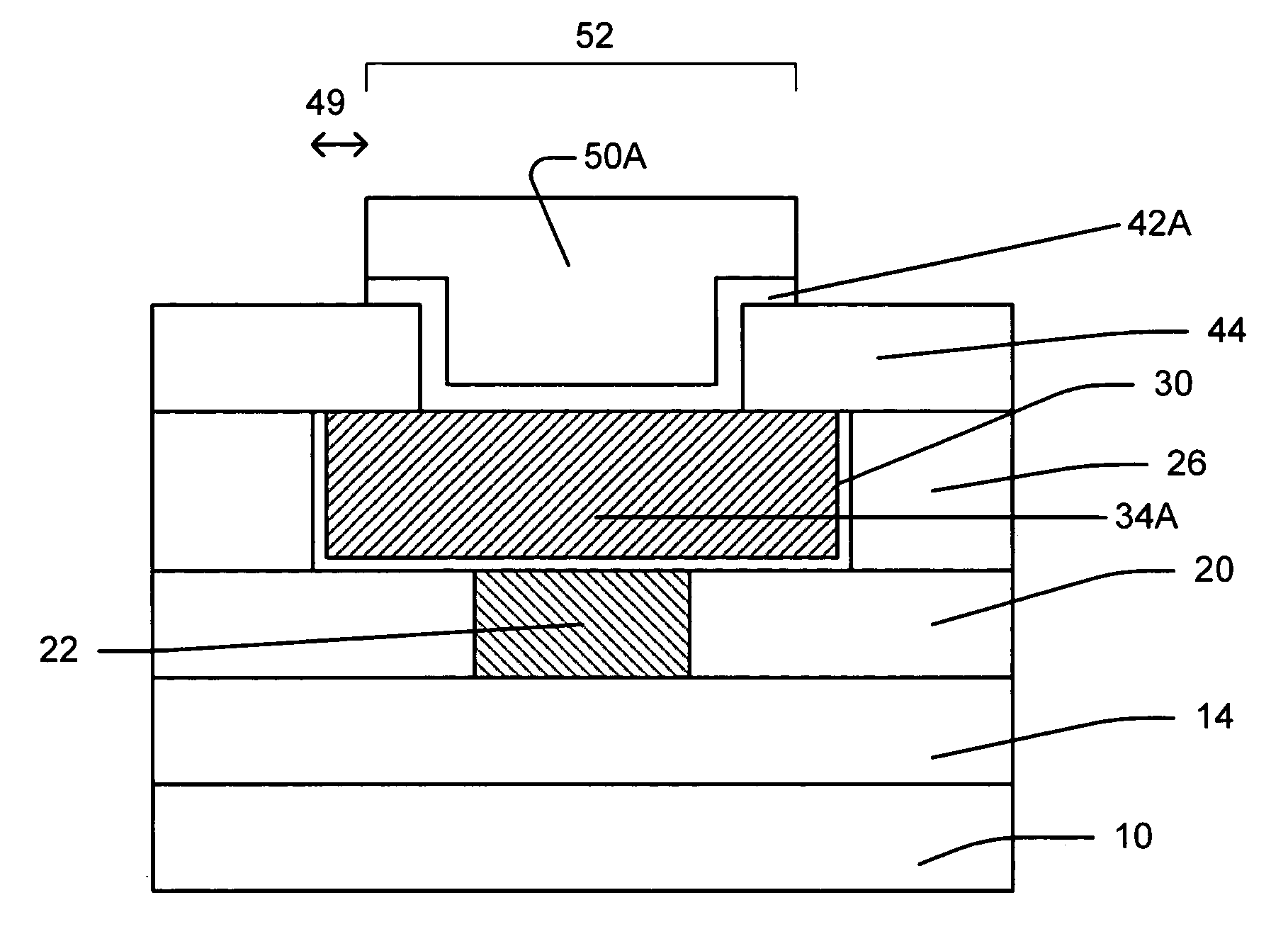
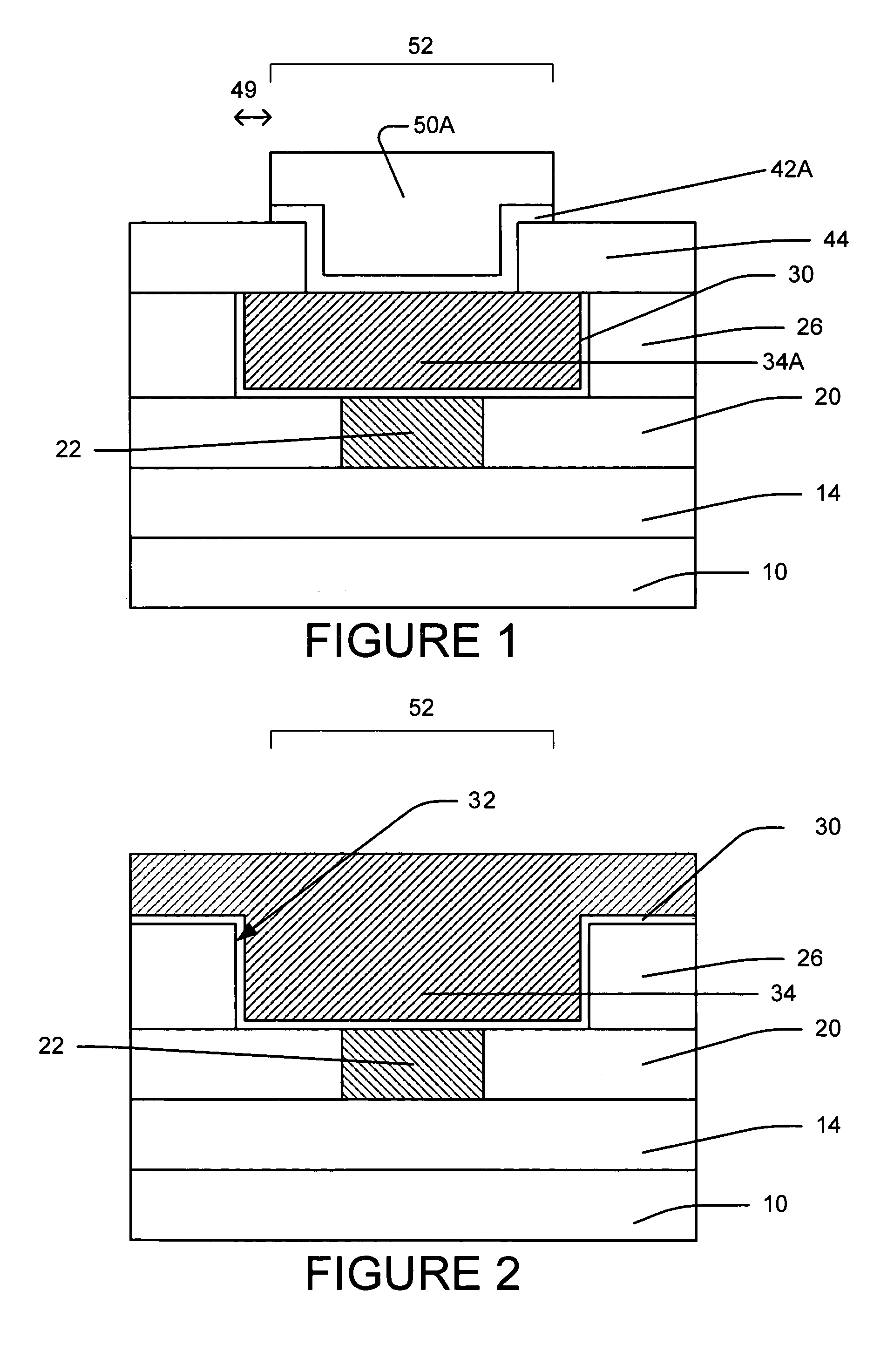
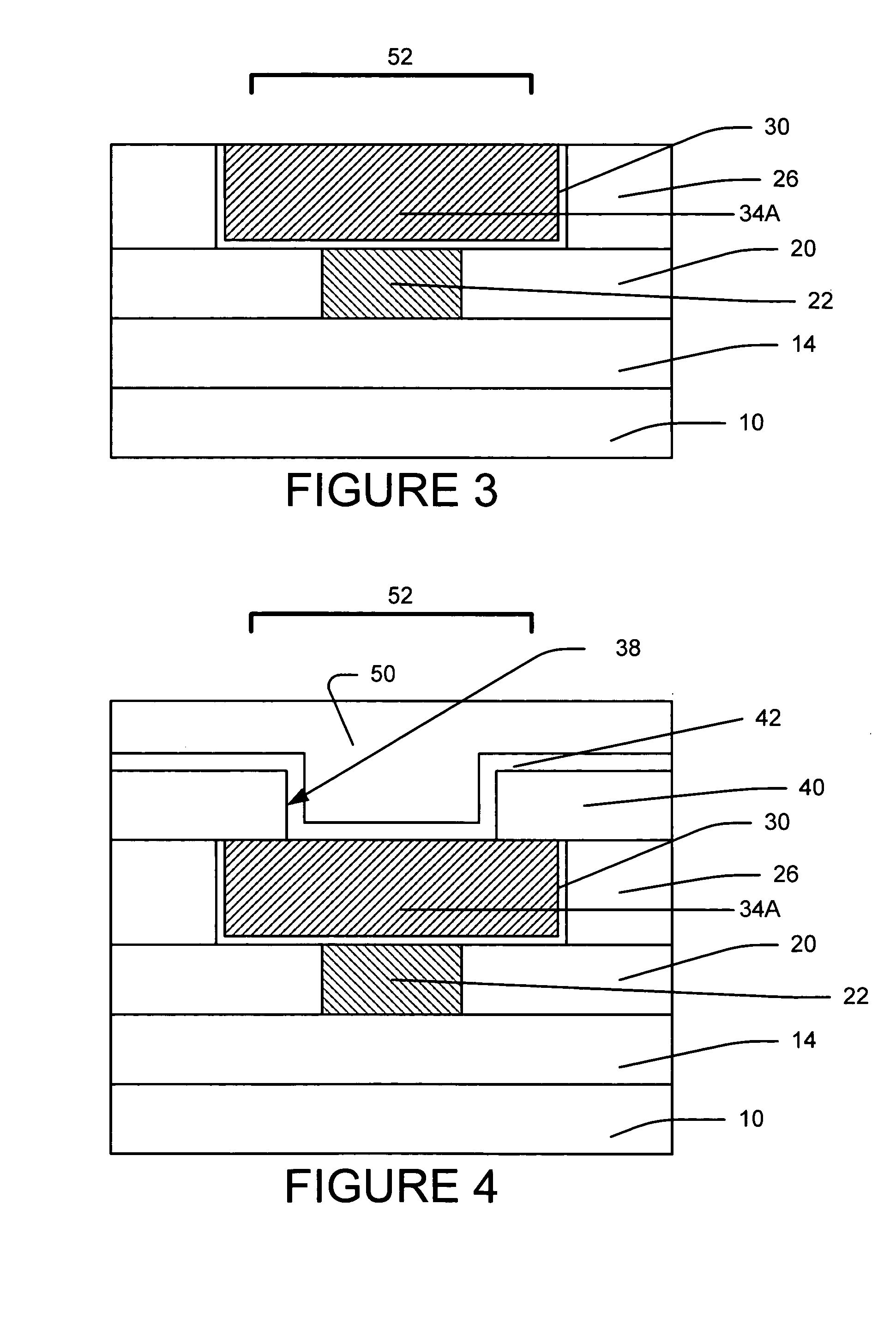
[0023]Introduction

[0024]New wire bonding processes and Low K dielectric layers under the bond pads have raised the stress requirement for bond pads. With the semiconductor technology move on to Cu / Low K integration, wire-bonding became one of the challenges due to the low modulus and fracture toughness of low K materials.

[0025]The inventors have found an improved bond pad structure is needed because (1) particular Low K dielectric are being used that have lower mechanical strength compared to SiO2 and 2) the wire bonding process are putting increased stress on bond pad and chips.

[0026]The wafers are often built up to 6 layers of Cu separated by Low K dielectrics, which themselves must be surrounded by diffusion barriers. In wire bonding, mechanical loading and ultra-sonic stresses applied by the tip of the bonding capillary to the bond-pad could also transmit to the underlying Cu / Low K stacks. Since Low K materials are not strong enough, bond-pad deformation or sinking could normall...


PUM


Abstract

A structure and method for an improved a bond pad structure. We provide a top wiring layer and a top dielectric (IMD) layer over a semiconductor structure. The buffer dielectric layer is formed over the top wiring layer and the top dielectric (IMD) layer. We form a buffer opening in the buffer dielectric layer exposing at least of portion of the top wiring layer. We form a barrier layer over the buffer dielectric layer, and the top wiring layer in the buffer opening. A conductive buffer layer is formed over the barrier layer. We planarize the conductive buffer layer to form a buffer pad in the buffer opening. We form a passivation layer over the buffer pad and the buffer dielectric layer. We form a bond pad opening in the passivation layer over at least a portion of the buffer pad. We form a bond pad support layer over the buffer pad and the buffer dielectric layer. We form a bond pad layer over the a bond pad support layer. The bond pad layer and the bond pad support layer are patterned to form a bond pad and bond pad support.

Description

BACKGROUND OF INVENTION[0001]1) Field of the Invention[0002]The present invention generally relates to a semiconductor device, and more specifically, to a bonding pad electrode structure and to a bond pad structure that prevents generation of cracks derived from mechanical stress from wire bonding.[0003]2) Description of the Related Art[0004]Integrated circuits must be electrically contacted. The electrical connection from the external pins of the integrated circuit package to the integrated circuit goes through bond pads which are located on the periphery of the integrated circuit. The bond pads are metal areas which are electrically connected to the devices in the integrated circuit via and electrically conducting wiring layers (e.g., Metal layers). Due to conventional bonding technology used to, for example, attach wires to the bond pads and to design constraints, the bond pads have relatively large dimensions as compared to the device dimensions and occupy or cover a significant...

Claims


Application Information

Patent Timeline
Patent Type & Authority Patents(United States)
IPC IPC(8): H01L21/44H01L21/60H01L23/485H01L23/532H01L29/40
CPCH01L24/03H01L24/05H01L24/06H01L24/11H01L23/53223H01L2924/0002H01L2224/0401H01L2224/05572H01L2224/05559H01L2924/01033H01L2224/04042H01L2224/05624H01L2224/05647H01L2224/13099H01L2924/01005H01L2924/01006H01L2924/01013H01L2924/01014H01L2924/01022H01L2924/01029H01L2924/01073H01L2924/01074H01L2924/01082H01L2924/05042H01L2924/14H01L2924/01019H01L2924/01024H01L2224/05552
Inventor FAN, ZHANGCHAO, ZHANG BEIWUPING, LIULIEP, CHOK KHOCHOO, HSIA LIANGKHENG, LIM YEOWCUTHBERTSON, ALANBOON, TAN JUAN
Owner CHARTERED SEMICONDUCTOR MANUFACTURING
Why Eureka
Try Eureka