Integrated schottky diode using buried power buss structure and method for making same

a power buss and integrated technology, applied in the field of schottky diodes, can solve the problems of lower breakdown, higher capacitance, and large leakage, and achieve the effects of high resistivity, low forward drop, and high resistivity

Inactive Publication Date: 2006-02-21
MICREL
View PDF3 Cites 24 Cited by
  • Summary
  • Abstract
  • Description
  • Claims
  • Application Information

AI Technical Summary

Benefits of technology

[0010]An integrated Schottky diode and method of manufacture of such a diode is disclosed. In a first aspect, a Schottky diode comprises a semiconductor substrate. The semiconductor substrate includes a high resistivity N-type epitaxial layer (EPI) on the substrate region. The diode includes a plurality of guard rings in the EPI layer and a plurality of oxidized slots. Finally, the diode includes metal within the plurality of slots to form a Buried Power Buss (BPB). A portion of the metal is completely oxide isolated from the other elements of the diode as well as the rest of the active circuitry and passive circuitry within the integrated chip.
[0011]In a second aspect, a method for manufacturing an integrated Schottky diode comprises providing a substrate region and a buried N+ layer followed by a high resistivity N-type epitaxial (EPI) layer. The method also includes providing a plurality of guard rings in the EPI layer and providing a plurality of slots in the semiconductor substrate that is in contact with the EPI layer and the substrate region. The method further includes a plurality of oxidizing the slots and providing metal within the plurality of slots to form a Buried Power Buss structure. A portion of the metal is completely oxide isolated from the other elements of the diode as well as the other active and passive elements within the integrated structure. In this approach, oxide is removed from the bottom of slots over the buried layer to allow a row resistance contact to the buried layer. Accordingly, the system and method in accordance with the present invention a Schottky diode is provided that has low forward drop, low leakage at low and high voltages, has a restricted capacitance and has a high reverse breakdown voltage.

Problems solved by technology

However, the increase in size normally results in greater leakage, higher capacitance, and lower breakdown.
Leakage is the result of: 1) the large area required to reduce the resistance, 2) the resultant increase in edges, and depletion region of the larger junction, 3) surface effects caused by contamination that will normally increase due to the increase in area, 4) the sharp junction curvature to the surface that gives high reverse leakage at elevated voltages, 5) lower breakdown voltage, and 6) junction spreading as the voltage is increased, resulting in increased depletion region and its resultant increased leakage.
This approach has some issues with leakage due to the junction tending to move out and therefore create a larger depletion region which increases the “capture” leakage.

Method used


Image

  • Integrated schottky diode using buried power buss structure and method for making same
  • Integrated schottky diode using buried power buss structure and method for making same
  • Integrated schottky diode using buried power buss structure and method for making same

Examples


Embodiment Construction

[0019]The present invention relates generally to semiconductor devices and particularly to integrated Schottky diodes. The following description is presented to enable one of ordinary skill in the art to make and use the invention and is provided in the context of a patent application and its requirements. Various modifications to the preferred embodiment and the generic principles and features described herein will be readily apparent to those skilled in the art. Thus, the present invention is not intended to be limited to the embodiment shown but is to be accorded the widest scope consistent with the principles and features described herein.

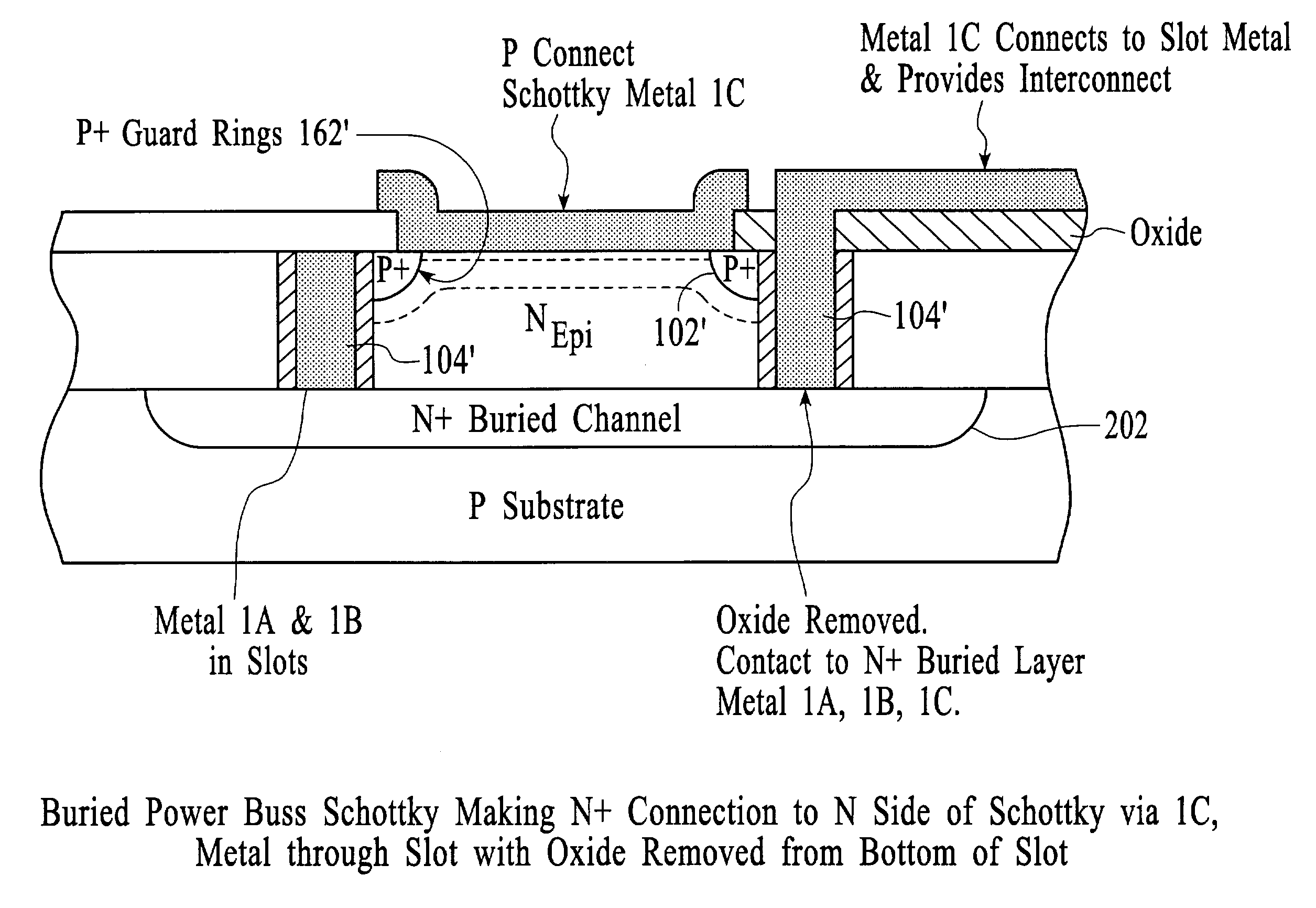
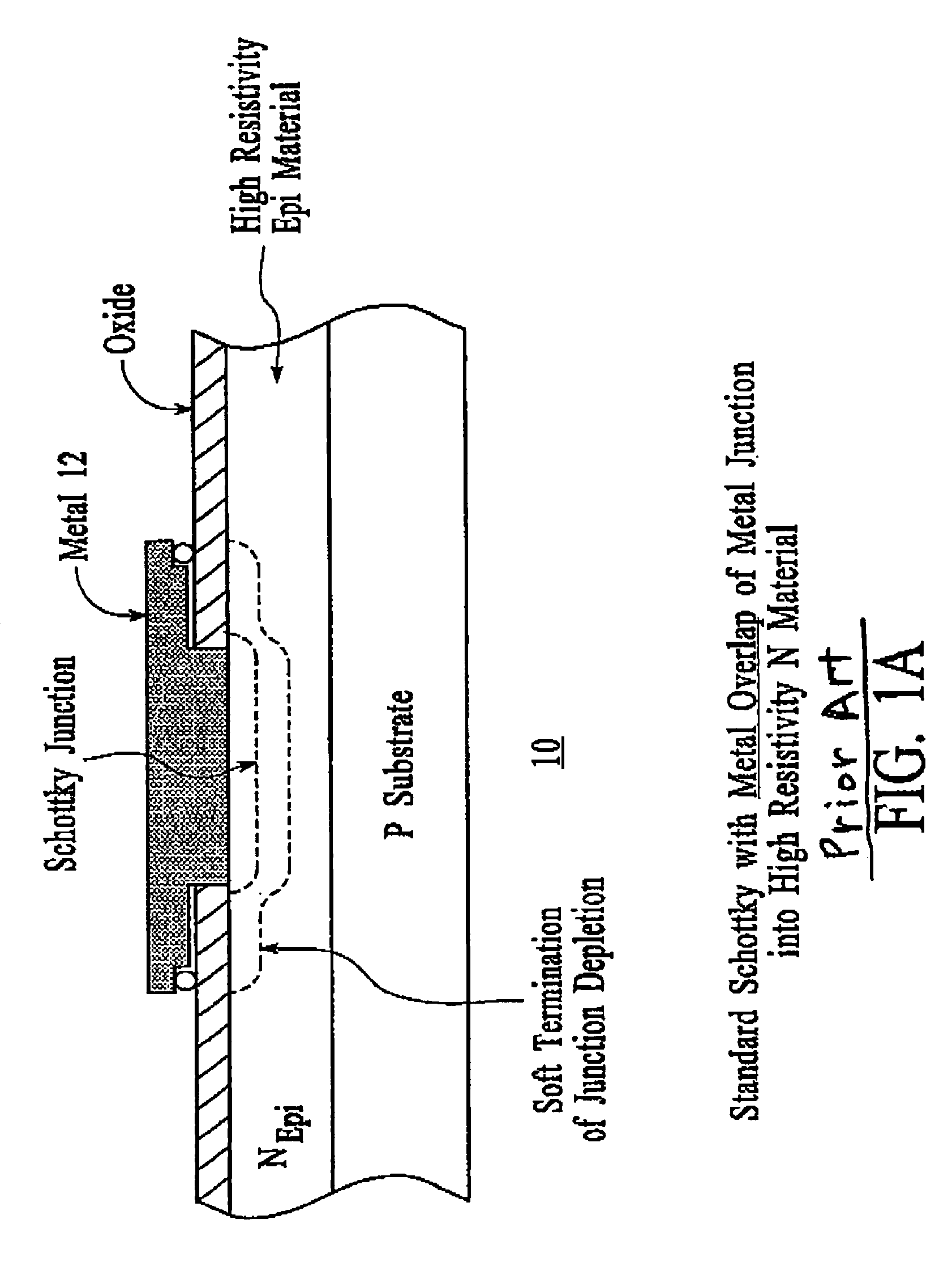
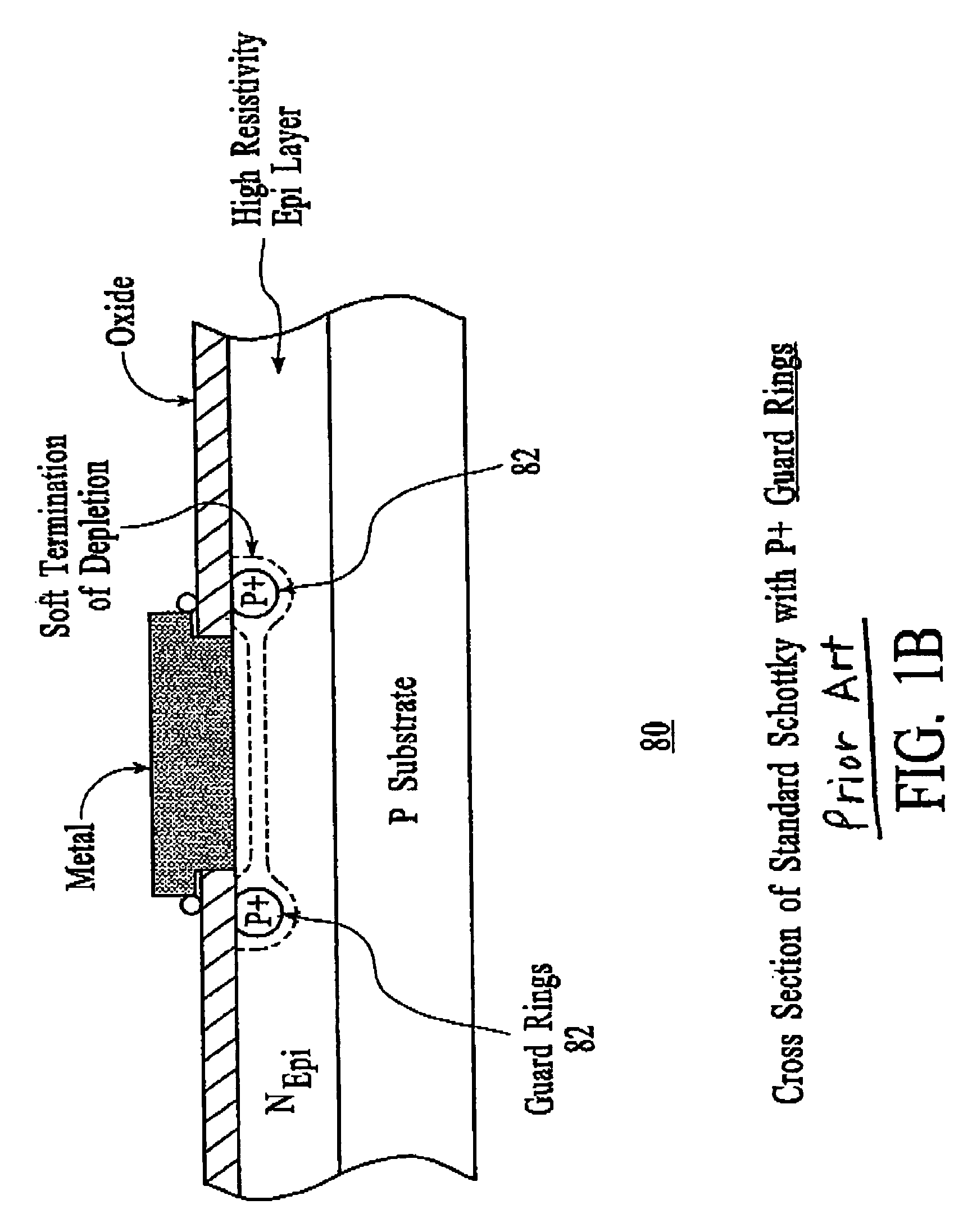
[0020]A system and method in accordance with the present invention utilizes the advantages described above in relation to the Schottky diodes of FIGS. 1–3 namely, it uses MOS type processing and surface improvement techniques to provide the proper surface; it uses overlapped Schottky metal; and it uses guard rings. Plus it adds another element—...


PUM


Abstract

An integrated Schottky diode and method of manufacture of such a diode is disclosed. In a first aspect, a Schottky diode comprises a semiconductor substrate. The semiconductor substrate includes an epitaxial layer (EPI) on the substrate region. The diode includes a plurality of guard rings in the EPI layer and a plurality of oxidized slots. Finally, the diode includes metal within the plurality of slots to form a Buried Power Buss. A portion of the metal is completely oxide isolated from the other elements of the diode. In a second aspect, a method for manufacturing a Schottky diode comprises providing a substrate region, A buried N+ region providing an epitaxial (EPI) layer. The method also includes providing a plurality of guard rings in the EPI layer and providing a plurality of slots in the semiconductor substrate that is in contact with the EPI layer and the substrate region. The method further includes a plurality of oxidizing the slots and providing metal within the plurality of slots to form a Buried Power Buss structure. A portion of the metal is completely oxide isolated from the other elements of the diode. Accordingly, the system and method in accordance with the present invention a Schottky diode is provided that has low forward drop, low leakage at low and high voltages, and has a high reverse breakdown voltage.

Description

FIELD OF THE INVENTION[0001]The present invention relates generally to semiconductor devices and particularly to Schottky diodes.BACKGROUND OF THE INVENTION[0002]The ideal Schottky diode in an integrated circuit would be one with low forward drop, low leakage, low capacitance and high breakdown. In general, this dictates a large area device to obtain the low forward drop by lowering the resistance due to spreading resistance effects, contact resistance and some depletion edge resistance. However, the increase in size normally results in greater leakage, higher capacitance, and lower breakdown.[0003]Leakage is the result of: 1) the large area required to reduce the resistance, 2) the resultant increase in edges, and depletion region of the larger junction, 3) surface effects caused by contamination that will normally increase due to the increase in area, 4) the sharp junction curvature to the surface that gives high reverse leakage at elevated voltages, 5) lower breakdown voltage, an...

Claims


Application Information

Patent Timeline
Patent Type & Authority Patents(United States)
IPC IPC(8): H01L29/74H01L21/00H01L21/28
CPCH01L29/872H01L21/74
Inventor HUSHER, JOHN DURBIN
Owner MICREL
Why Eureka
Try Eureka