RF passive circuit and RF amplifier with via-holes

a passive circuit and passive circuit technology, applied in the direction of waveguides, basic electric elements, waveguide type devices, etc., can solve the problems of large space occupation and inability to reduce the size of the conventional type of rf amplifier and rf passive circuit, and achieve the effect of reducing the occupancy of the passive circuit and reducing the size of the passive circui

Inactive Publication Date: 2006-02-28
PANASONIC CORP
View PDF9 Cites 32 Cited by
  • Summary
  • Abstract
  • Description
  • Claims
  • Application Information

AI Technical Summary

Benefits of technology

[0027]The above structure enables to incorporate a capacitor in a via-hole, thereby enabling a three-dimensional location of the following three elements on one semiconductor substrate; a spiral inductor, a capacitor, and a via-hole. Thus reduced occupancy will produce an effect of enabling a smaller RF passive circuit and an RF amplifier made of the RF passive circuits as main components.
[0030]This structure will help to make a smaller RF passive circuit and a smaller RF amplifier by enabling a three-dimensional location of a spiral inductor, a capacitor, and a via-hole. Moreover, a static capacity will be increased without increasing the occupancy, which will facilitate designing of such a circuit as a bias feeding circuit of an RF amplifier which inherently requires large capacity.
[0033]The above structure enables to accommodate a static capacity where the extended part of the metal layer and the spiral metal layer face each other with a dielectric layer in between. This realizes a three-dimensional location of a spiral inductor, a capacitor, and a via-hole, thereby reducing the occupancy thereof. This also helps to make a smaller RF passive circuit, and a smaller RF amplifier.
[0036]The above structure enables a three dimensional location of a spiral inductor, a capacitor, and a via-hole from inside to the surface of the semiconductor substrate, thereby reducing the occupancy thereof, and helps to make a smaller RF passive circuit and a smaller RF amplifier.
[0042]The above structure enables a three dimensional location of a capacitor and a via-hole on one semiconductor substrate, thereby reducing the occupancy thereof. This helps making a smaller RF passive circuit and a smaller RF amplifier.

Problems solved by technology

As seen above, the conventional type of RF amplifiers and RF passive circuits cannot be made smaller in size, due to the two-dimensional positioning of the constituting elements of the drain voltage feeding circuit 807, which inherently take much space.

Method used


Image

  • RF passive circuit and RF amplifier with via-holes
  • RF passive circuit and RF amplifier with via-holes
  • RF passive circuit and RF amplifier with via-holes

Examples


first embodiment

1. First Embodiment

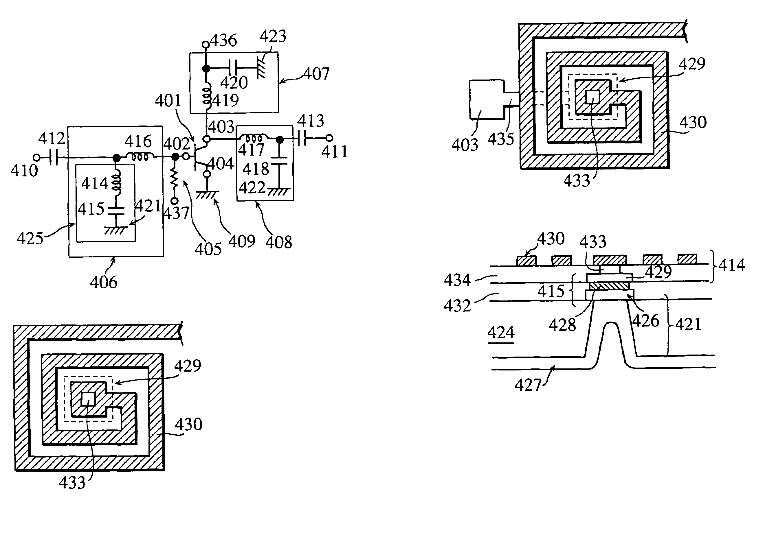
[0056]FIGS. 1A–1D are drawn to describe the first embodiment of the present invention.

[0057]FIG. 1A is a schematic circuit diagram of the RF amplifier and the RF passive circuit that the present invention is applied to. The circuit is basically the same as the one in FIG. 8A, with minor difference in reference numbers for parts and materials. Therefore description is omitted.

[0058]FIGS. 1B and 1C are both diagrams showing a plan view of structures realized by an input matching circuit portion 125 and a drain voltage feeding circuit 107 in FIG. 1(1), pertaining to the first embodiment.

[0059]FIG. 1B is a plan view of the input matching circuit portion 125. An input matching parallel inductor 114 is in a spiral-electrode-pattern, and an input matching parallel capacitor 115 is an MIM capacitor and is created inside an input matching circuit via-hole 121, which is a surface via-hole made from the front surface of the GaAs substrate 124.

[0060]The following is a detaile...

second embodiment

2. Second Embodiment

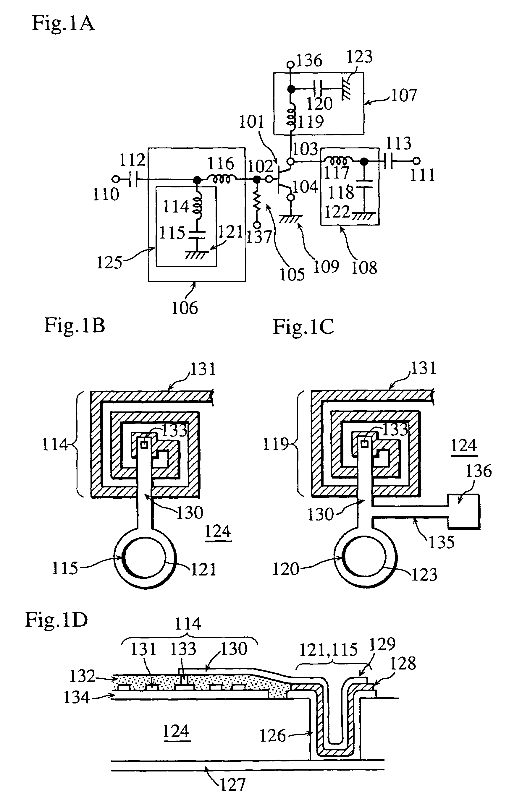
[0066]FIGS. 2A–2D are drawings depicted for the explanation of the second embodiment of the present invention. The application circuits will not be described since they are the same as those of FIG. 1A. FIG. 2B depicts an input matching circuit, and FIG. 2C depicts a drain voltage feeding circuit. FIG. 2D is a cross-sectional view of both circuits.

[0067]The second embodiment has larger static capacity than the first embodiment, realized by an input matching parallel capacitor 221 created inside a via-hole 215. That is, the second embodiment has a five-layer film inside the via-hole 215 made by stacking: a ground metal layer 226, a first dielectric layer 2281, a first wiring metal layer for capacity element 2291, a second dielectric layer 2282, and a second wiring metal layer for capacity element 2292, from the bottom. Note that the three metal layers are made of the same metal material, which is the same material used in the first embodiment. Likewise, all the tw...

third embodiment

3. Third Embodiment

[0069]FIGS. 3A–3C are depicted for the explanation of the third embodiment.

[0070]FIG. 3A is a plan view showing a schematic circuit diagram for an RF amplifier the third embodiment is applied to. The circuits are the same as those depicted in FIG. 8A, whose description is omitted accordingly.

[0071]FIG. 3B shows a plan view of an input matching circuit portion 325 and a drain voltage feeding circuit 307, both as parts of an RF amplifier of the third embodiment. FIG. 3C is a cross-sectional view of FIG. 3B.

[0072]The following focuses on the input matching circuit portion 325 for detailed description.

[0073]First, a first wiring metal layer 330 is formed by gold / titanium vacuum evaporation in a spiral pattern seen from the above; it is formed so as to cover an insulator film 334 made of such materials as silicon oxide on a GaAs substrate 324. Next, a dielectric layer 328 made of titanium oxide strontium which has a permittivity of 100 or more is applied on the first w...


PUM


Abstract

An input matching parallel inductor 114 which utilizes a spiral inductor, and an input matching parallel capacitor 115 which utilizes an MIM capacitor, both being constituting elements of an input matching circuit portion 125, form an input matching parallel capacitor 115 inside an input matching circuit via-hole 121 being formed by applying a method of surface via-hole to the front surface of a GaAs substrate 124. A choke inductor 119 which utilizes a spiral inductor, and a bypass capacitor 120 which utilizes an MIM capacitor, both being constituting elements of a drain voltage feeding circuit 107, form a bypass capacitor 120 inside a drain voltage feeding circuit via-hole 123 formed by applying a method of surface via-hole to the front surface of the GaAs substrate 124. A drain voltage terminal 136 is extended by a drawing wire 135 from between the spiral inductor and the drain voltage feeding circuit via-hole 123.

Description

[0001]This is a divisional application of U.S. Ser. No. 09 / 928,733, filed on Aug. 13, 2001 now U.S. Pat. No. 6,800,920.BACKGROUND OF THE INVENTION[0002](1) Field of the Invention[0003]This invention relates to a technology for making smaller and lighter RF passive circuits and RF amplifiers equipped with via-holes.[0004](2) Prior Art[0005]Recently, various types of mobile communication tools, such as portable phones or portable information terminals have been commercialized all over the world. As portable phones, cellular phones for bands of 900 MHz and 1.5 GHz, and Personal Handyphone System (PHS) for a band of 1.9 GHz are two examples that are commercialized in Japanese market. Other examples include world-famous GSM, and CDMA among the technologies adopted in PCS (Personal Communications Services) in the U.S.A.[0006]As a third-generation mode following the analogue mode and the digital mode, IMT2000 is planned to be commercialized in the future.[0007]In developing mobile communic...

Claims


Application Information

Patent Timeline
Patent Type & Authority Patents(United States)
IPC IPC(8): H01L29/00H01L23/522H01P3/08H01L23/66H03F1/56H03F3/191H03F3/193H03F3/60
CPCH01L23/5223H01L23/5227H01L23/642H01L23/645H01L23/66H01L27/016H03F1/565H03F3/191H01L2924/0002H01L2223/6655H01L2924/19015H01L2924/3011Y10S438/957H01L2924/00
Inventor NISHIJIMA, MASAAKI
Owner PANASONIC CORP
Why Eureka
Try Eureka