

Semiconductor device and fabrication process thereof
a semiconductor and semiconductor technology, applied in semiconductor devices, semiconductor/solid-state device details, electrical devices, etc., can solve the problems of inability to achieve necessary alignment, reduce the mark correspondingly, and the device isolation structure cannot provide the desired device isolation performan
- Summary
- Abstract
- Description
- Claims
- Application Information
AI Technical Summary
Benefits of technology
Problems solved by technology
Method used
Image

Examples
first embodiment
[First Embodiment]
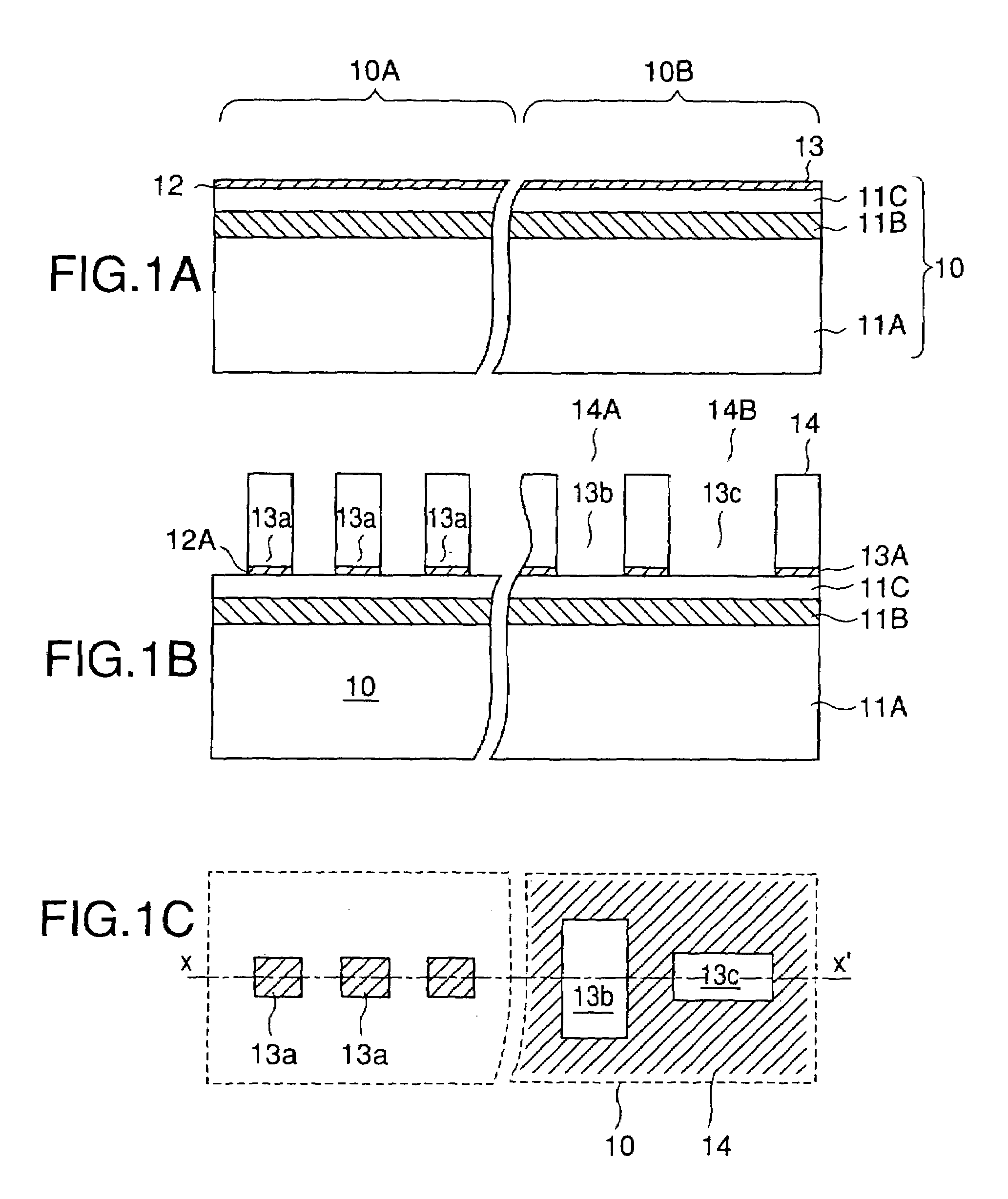
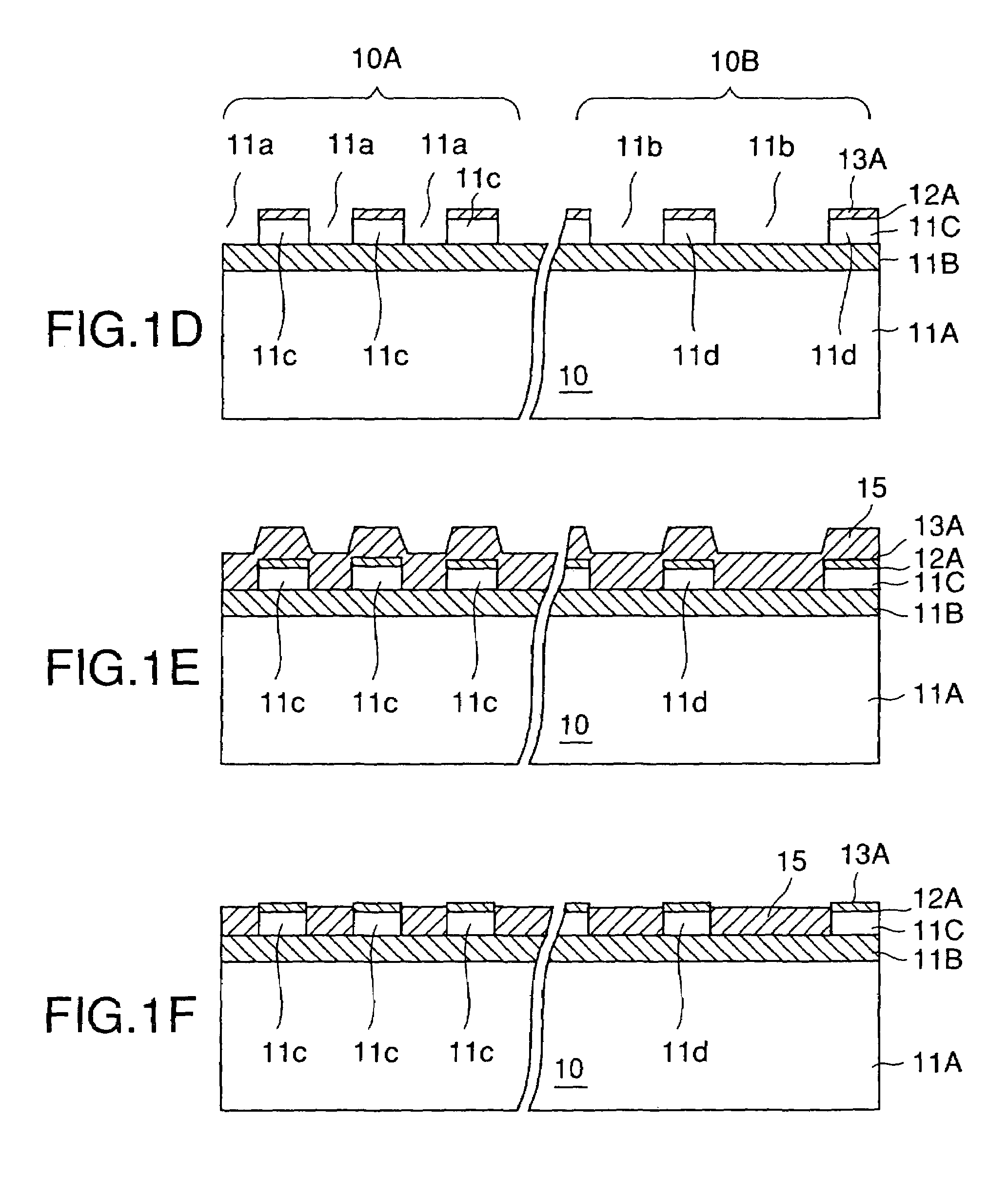
[0060]Next, the fabrication process of a semiconductor device according to a first embodiment of the present invention will be explained with reference to FIGS. 5A–5K, wherein it should be noted that FIG. 5A is a cross-sectional view taken along a line x–x′ of FIG. 5B, while FIG. 5C is a cross-sectional view taken along a line x–x′ of FIG. 5D.
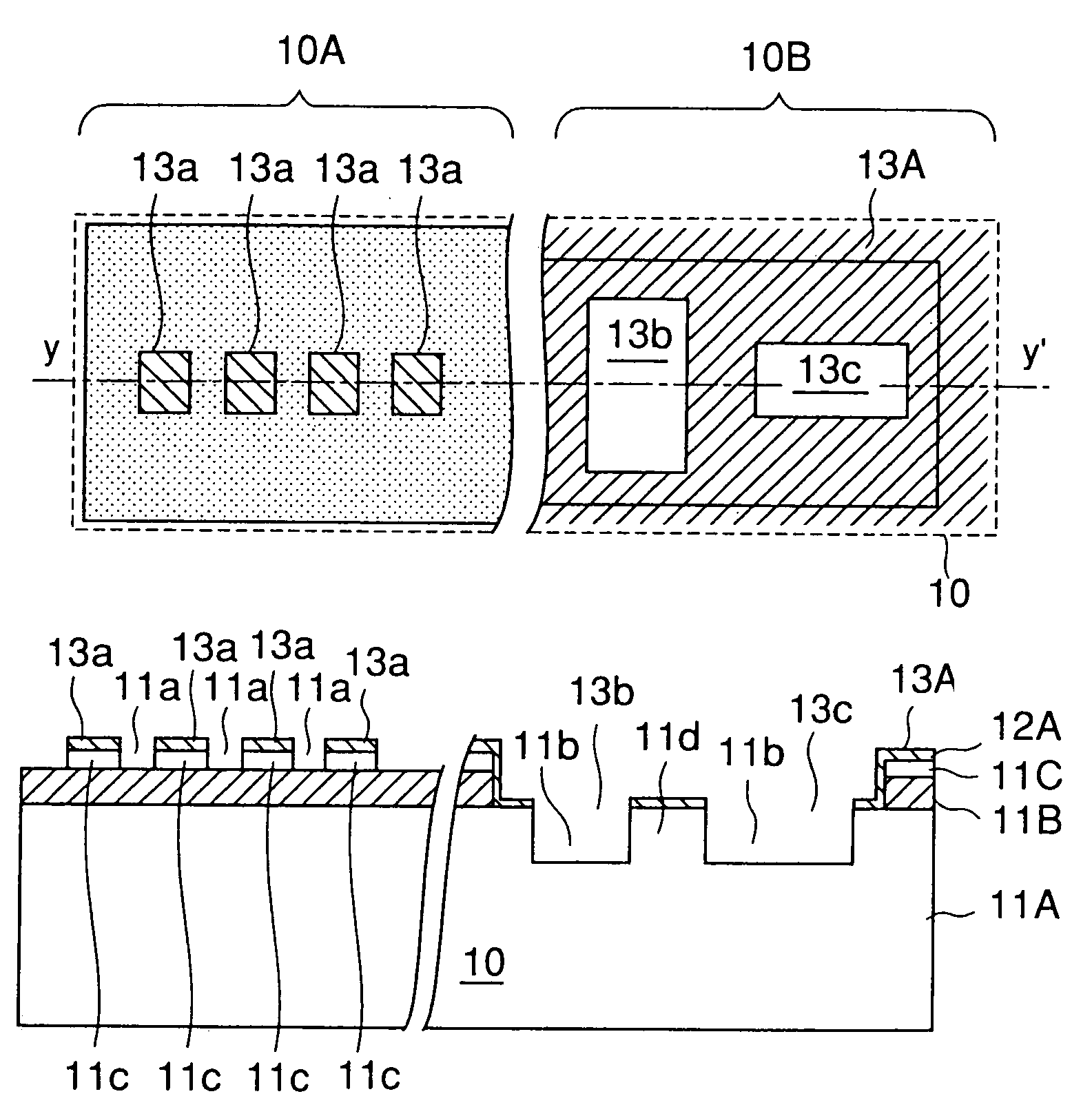
[0061]Referring to FIG. 5A, the SOI substrate 20 may be formed by a process such as a SIMOX process and includes a Si support substrate 21A on which an SiO2 buried insulation layer 21B is formed with a thickness of about 400 nm. Further, an active layer 21C of single crystal Si is formed on the SiO2 buried insulation layer 21B with a thickness of about 150 nm. On the SOI substrate 20, there are formed a device array region 20A and an alignment mark formation region 20B such that a device region and a device isolation region are formed in the device array region 20A and an alignment mark is formed in the alignment mark formatio...
second embodiment
[Second Embodiment]
[0072]Next, a process of fabricating a semiconductor device according to a second embodiment of the present invention will be explained with reference to FIGS. 6A–6L, wherein those parts explained previously are designated by the same reference numerals and the description thereof will be omitted.
[0073]Referring to FIGS. 6A and 6B at first, an SiN film 23 is deposited on the SOI substrate 20 explained previously with reference to FIG. 5A in the present embodiment by a CVD process, and the like, so as to cover the SiO2 film 22. Further, a resist pattern 25 explained previously with reference to FIG. 5C is formed on the SiN film 23. Further, the SiN film 23 and also the SiO2 film 22 underneath the SiN film 23 are patterned by using the resist pattern as a mask, and as a result, there are formed the SiN patterns 23A in the device array region 20A and the openings 23B and 23C are formed in the SiN layer 23 in the alignment mark formation region 20B respectively in cor...
third embodiment
[Third Embodiment]
[0086]Next, the process of fabricating a semiconductor device according to a third embodiment of the present invention will be explained with reference to FIGS. 7A–7H, wherein those parts explained previously are designated by the same reference numerals and the description thereof will be omitted.
[0087]Referring to the drawings, The steps from FIGS. 7A to 7C are identical with the steps of FIGS. 6A to 6C of the previous embodiment, and the SiO2 film 26 is deposited on the structure of FIG. 7C by a CVD process in the step of FIG. 7D so that the SiO2 film 26 buries the device isolation trench 21b and also the grooves 21c and 21d.
[0088]Further, in the step of FIG. 7E, the SiO2 film 26 is removed by polishing, by using a CMP process, until the SiN film 23 or the SiN pattern 23A is exposed. As a result of the process of FIG. 7E, there is obtained a structure in which the device isolation grooves 21b formed between the device regions 21a (see FIG. 6C) are filled with t...
PUM
 Abstract
Description
Claims
Application Information