Hybrid buried/ridge planar waveguides

a planar waveguide and buried/ridge technology, applied in the field of optical waveguide devices, can solve the problems of increasing the difficulty of forming coupling regions, the conflicting requirements of the different components of the device, and the loss of bending in the ring will be too high, so as to achieve the effect of easy integration of waveguide devices, high device packing densities, and improved device performan

Inactive Publication Date: 2006-02-28
GOOGLE LLC
View PDF10 Cites 14 Cited by
  • Summary
  • Abstract
  • Description
  • Claims
  • Application Information

AI Technical Summary

Benefits of technology

[0015]The invention thus enables fabrication on a single chip of an optical device having a mixture of high and low index contrast waveguide sections, thus allowing independent optimisation of parts of the device which had irreconcilable design requirements in prior art fabrication methods.
[0016]Further, the invention allows low-loss bends, such as L-bends or U-bends to be made wherever desired on a chip by removing material to form an exposed ridge section, thereby allowing better use of the space available on a chip. Higher device packing densities are thus easily achievable in integrated waveguide devices. In one example described further below, ridge section U-bends are used to form a multiple cascade of Mach-Zehnder interferometers made out of buried waveguide sections.
[0017]A transition section is advantageously arranged between a buried and ridge waveguide section to provide very low transition losses. The transition section can be formed by tapering, preferably adiabatically, the lateral dimensions of the cladding layer beside the core of the waveguide so that the lateral cladding thickness increases from a low (possibly zero) value in the ridge section to a high (typically effectively infinite) value in the buried waveguide section. In this context, ‘effectively’ infinite is meant to describe that the lateral cladding thickness is sufficiently large that substantially no field of the fundamental waveguide mode extends beyond the lateral cladding. With this tapered transition section, coupling of the respective propagation modes in the buried and ridged waveguide sections is effected by mode adaptation in the transition section.
[0021]According to a first aspect of the invention, there is provided an optical device comprising a waveguide having a core extending in a plane between a buried section of the waveguide lying below an upper surface of the optical device and a ridge section of the waveguide having side surfaces extending below the upper surface beside the core, thereby to provide enhanced lateral confinement of waveguide modes in the ridge section.
[0024]A transition section may be provided interconnecting the buried and ridge sections, the transition section comprising lateral cladding having a width that increases from the ridge section to the buried section to increase the effective refractive index of the fundamental mode of the waveguide from a lower value in the ridge section to a higher value in the buried section. The cladding width may be varied adiabatically in the transition section, thereby to suppress transition losses.
[0027]According to a second aspect of the invention there is provided a method of fabricating a waveguide structure starting from a buried waveguide structure comprising a buried waveguide core lying below an upper surface, the method comprising removal of parts of the buried waveguide structure beside the core to form a ridge containing the core, thereby creating a hybrid buried / ridge waveguide structure having a continuous common core with enhanced lateral confinement of waveguide modes in the ridge.

Problems solved by technology

If such a device is to be made integrated on a single chip or substrate, there is then the problem of how to satisfy the conflicting requirements of the different components of the device.
In this case, the coupling region is increasingly difficult to fabricate as the index contrast increases, whereas without sufficient index contrast bending losses in the ring will be too high.
However, because of the low refractive index contrast of such devices, the minimum bend radius achievable is quite large, being several millimetres, and the free spectral range (FSR) is consequently quite small, for example only a few GHz using conventional glass on silicon technology with an index contrast of 0.7% (e.g. 8–12.5 GHz in reference [10]).
However, such waveguides are less than half a micrometer wide and present very high propagation and fibre-coupling losses.
The realisation of a good quality directional coupler is a critical issue in high index contrast waveguides, such as these deep etched GaAs / AlGaAs waveguides.
However, these methods require two steps of both deposition and etch of the waveguide core, and the alignment of the second waveguide core to the first one is very critical.
But the higher the order of the filter the longer the device.
However, there is always a limited wafer size in an integrated optic process, which may limit the number of stages of the filter.
But this is not generally possible, since a device component such as a Mach-Zehnder interferometer needs a low index contrast fabrication for good quality, which in turn precludes being able to provide low-loss bent waveguides with a small enough bend radius.
For waveguide devices, high packing densities will be difficult to achieve without low-loss tight waveguide bends.

Method used


Image

  • Hybrid buried/ridge planar waveguides
  • Hybrid buried/ridge planar waveguides
  • Hybrid buried/ridge planar waveguides

Examples


Embodiment Construction

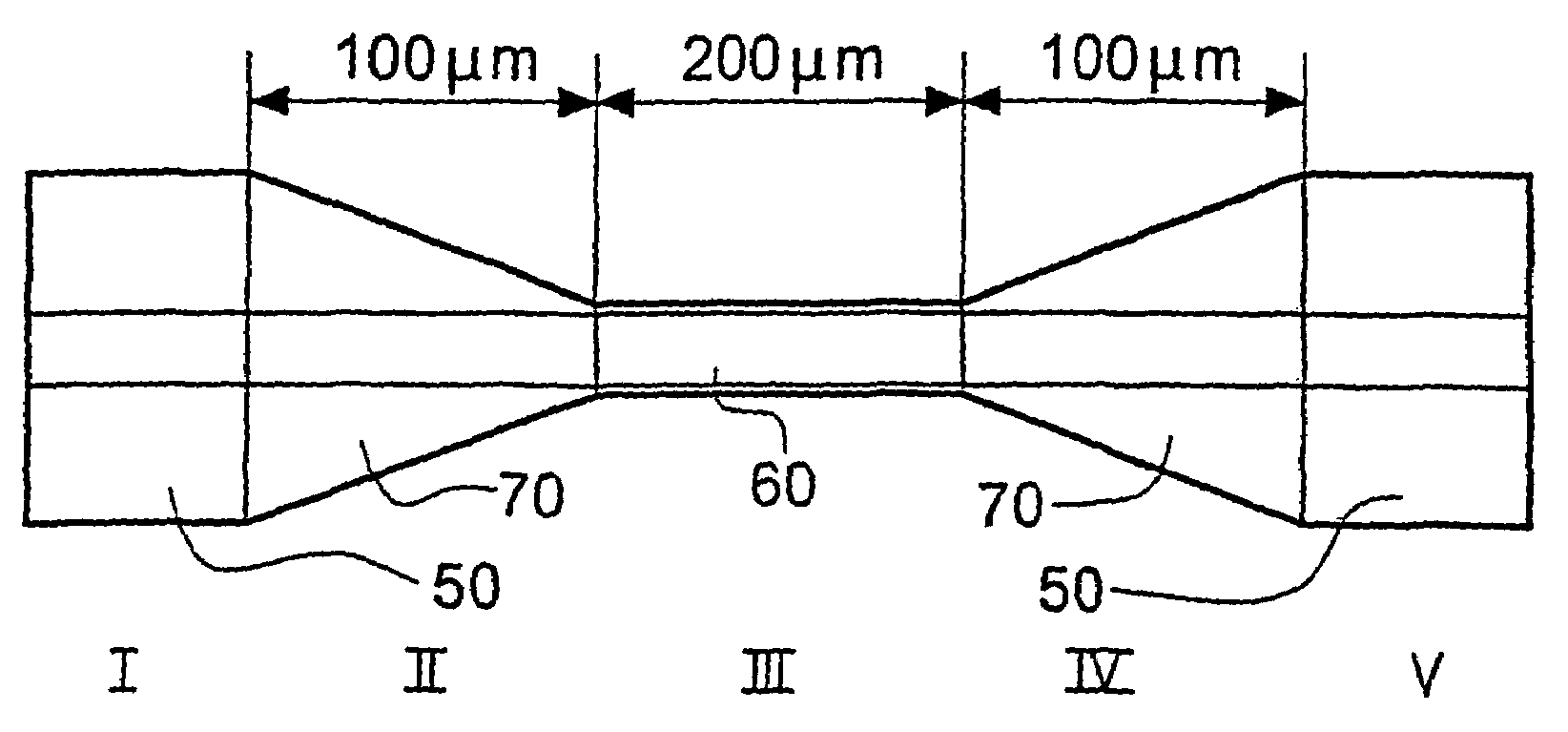
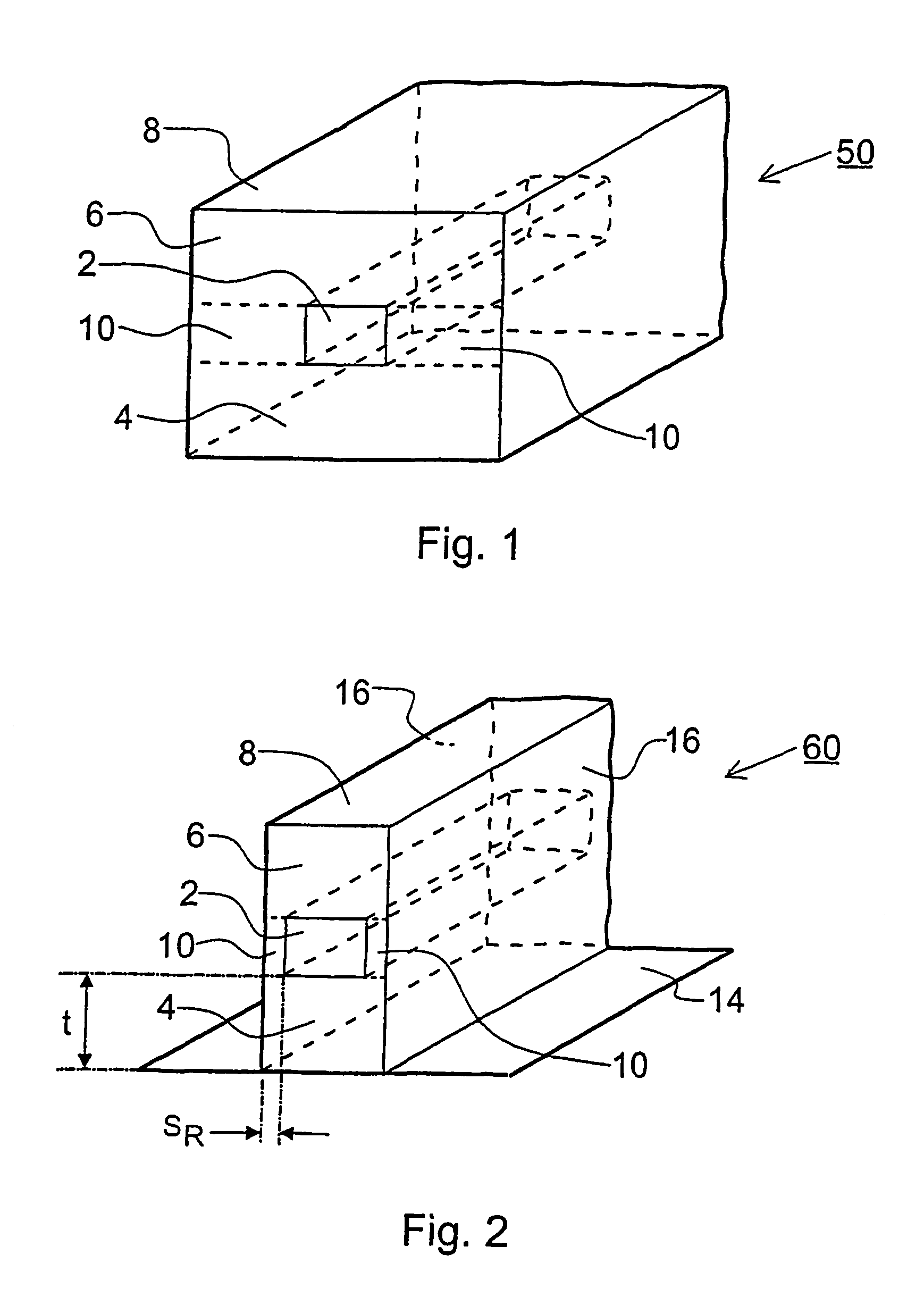
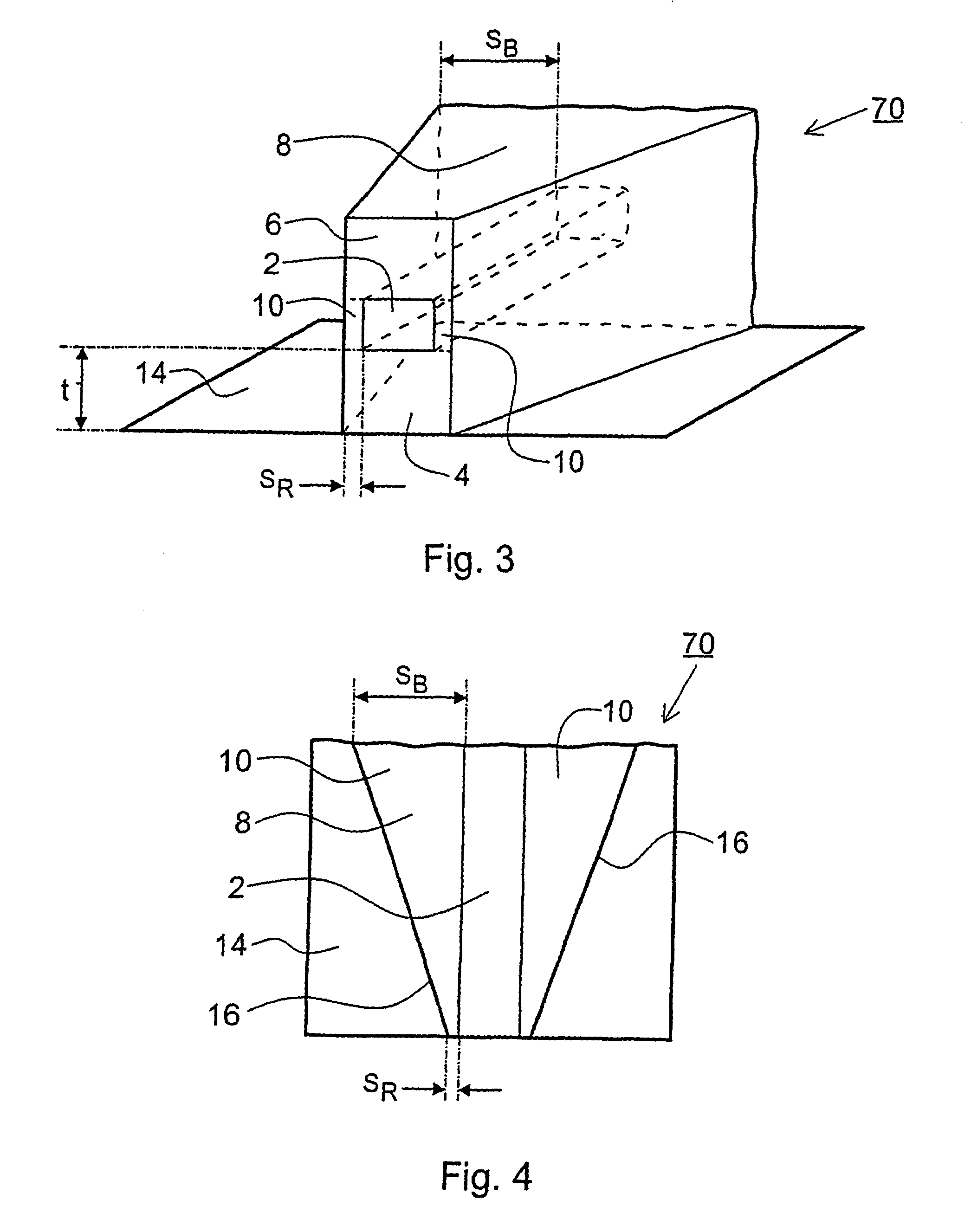
[0049]FIG. 1 is a schematic perspective of a buried waveguide section 50 which forms component part of an optical device of a first embodiment of the invention. In this embodiment the example of a glass waveguide realised by silica on silicon fabrication is taken. The silica is doped with Ge to provide the desired level of refractive index contrast. Other dopants could be used in alternative embodiments. The buried waveguide section comprises a generally rectangular section core 2 extending in a plane beneath an upper surface 8 and surrounded by cladding material built up from an upper cladding layer 6, a lower cladding layer 4 and two lateral cladding layers 10 on either side of the core 2. The silica waveguide structure is arranged on a silicon substrate (not shown). In alternative embodiments, other substrates such as glass (doped or undoped) may be used. The main role of the substrate is to provide mechanical support. In this example of silica on silicon, the physical parameters...


PUM


Abstract

A hybrid waveguide structure having a combination of buried waveguide sections and ridge waveguide sections on the same substrate, share a common core layer. The buried waveguide sections provide the low index contrast desirable for couplers and other device components. The ridge waveguide sections provide the high index contrast needed for efficient low-loss tightly curved waveguides. The devices are fabricated starting from a low index contrast buried waveguide. Cladding material is then selectively removed by etching down from an upper surface either side of the waveguide core to a lower surface. This forms an enhanced index contrast ridge section of the waveguide. The other sections of the waveguide core remain buried and thus retain lower index contrast. Using this approach, a variety of optical devices, such as add / drop or add-after-drop multiplexers for WDM applications based on microrings or Mach-Zehnder interferometers, can be made with large feature sizes of several microns using silica-on-glass or silica-on-silicon technology, for example, and without having to use nanofabricated semiconductor structures.

Description

CROSS REFERENCE TO RELATED APPLICATIONS[0001]This application is a national phase application based on PCT / IB01 / 02725, filed Oct. 26, 2001, the content of which is incorporated herein by reference, and claims the priority of European Patent Application no. 00309508.0, filed Oct. 27, 2000, the content of which is incorporated herein by reference and claims the benefit of U.S. Provisional Application No. 60 / 244,926, filed Nov. 2, 2000, the content of which is incorporated herein by reference.BACKGROUND OF THE INVENTION[0002]The invention relates to optical waveguide devices and to methods of fabricating optical waveguide devices.[0003]In the realisation of passive integrated optical devices there is often a preferred waveguide structure for each of the building blocks of the device. For example, it is easier to fabricate a high quality directional coupler in a low refractive index contrast waveguide. Refractive index contrast, or index contrast for short, refers to the size of the ref...

Claims


Application Information

Patent Timeline
Patent Type & Authority Patents(United States)
IPC IPC(8): G02B6/10G02B6/12G02B6/122G02B6/125G02B6/34
CPCG02B6/12007G02B6/122G02B6/1228G02B6/125G02B6/29355G02B2006/12169G02B2006/12097G02B2006/121G02B2006/12159G02B6/29343
Inventor CARNIEL, FEDERICOCOSTA, RAFFAELLAMELLONI, ANDREA
Owner GOOGLE LLC
Why Eureka
Try Eureka