Thin leadless plastic chip carrier

a leadless, chip-carrying technology, applied in the direction of semiconductor devices, semiconductor/solid-state device details, electrical apparatus, etc., can solve the problems of lower electrical impedance and permit the operation of the package, and achieve the effect of reducing the length of the wire bonding to the contact pads, reducing the electrical impedance, and reducing the length of the wire bonding to the power ring and the die attaching pad (ground)

Active Publication Date: 2006-03-07
UTAC HEADQUARTERS PTE LTD
View PDF28 Cites 117 Cited by
  • Summary
  • Abstract
  • Description
  • Claims
  • Application Information

AI Technical Summary

Benefits of technology

[0010]Advantageously, a thin package profile is possible as the die attach pad is offset from the contact pads and protrudes from the molding compound. Because the die attach pad is offset from the contact pads, the semiconductor die sits in a pocket on the die attach pad. Thus, the length of the wire bonds to the contact pads, to the power ring and to the die attach pad (ground) is reduced. This results in lower electrical impedance and permits operation of the package at higher frequencies.
[0011]Also, because the die attach pad is offset and protrudes from the molding compound, more space is provided within the package to accommodate several semiconductor dice stacked on top of each other, without significantly increasing the package size over standard, single semiconductor die packages.

Problems solved by technology

This results in lower electrical impedance and permits operation of the package at higher frequencies.

Method used


Image

  • Thin leadless plastic chip carrier
  • Thin leadless plastic chip carrier
  • Thin leadless plastic chip carrier

Examples


Embodiment Construction

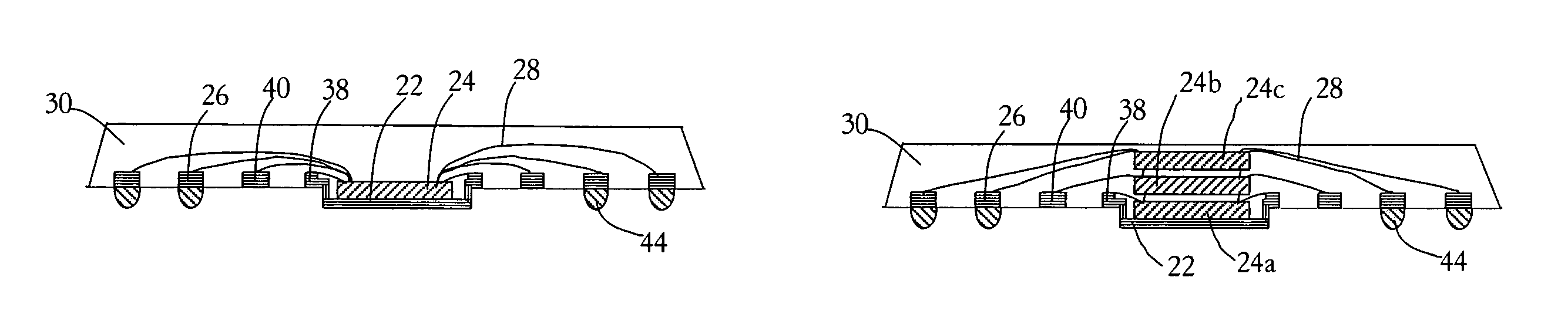
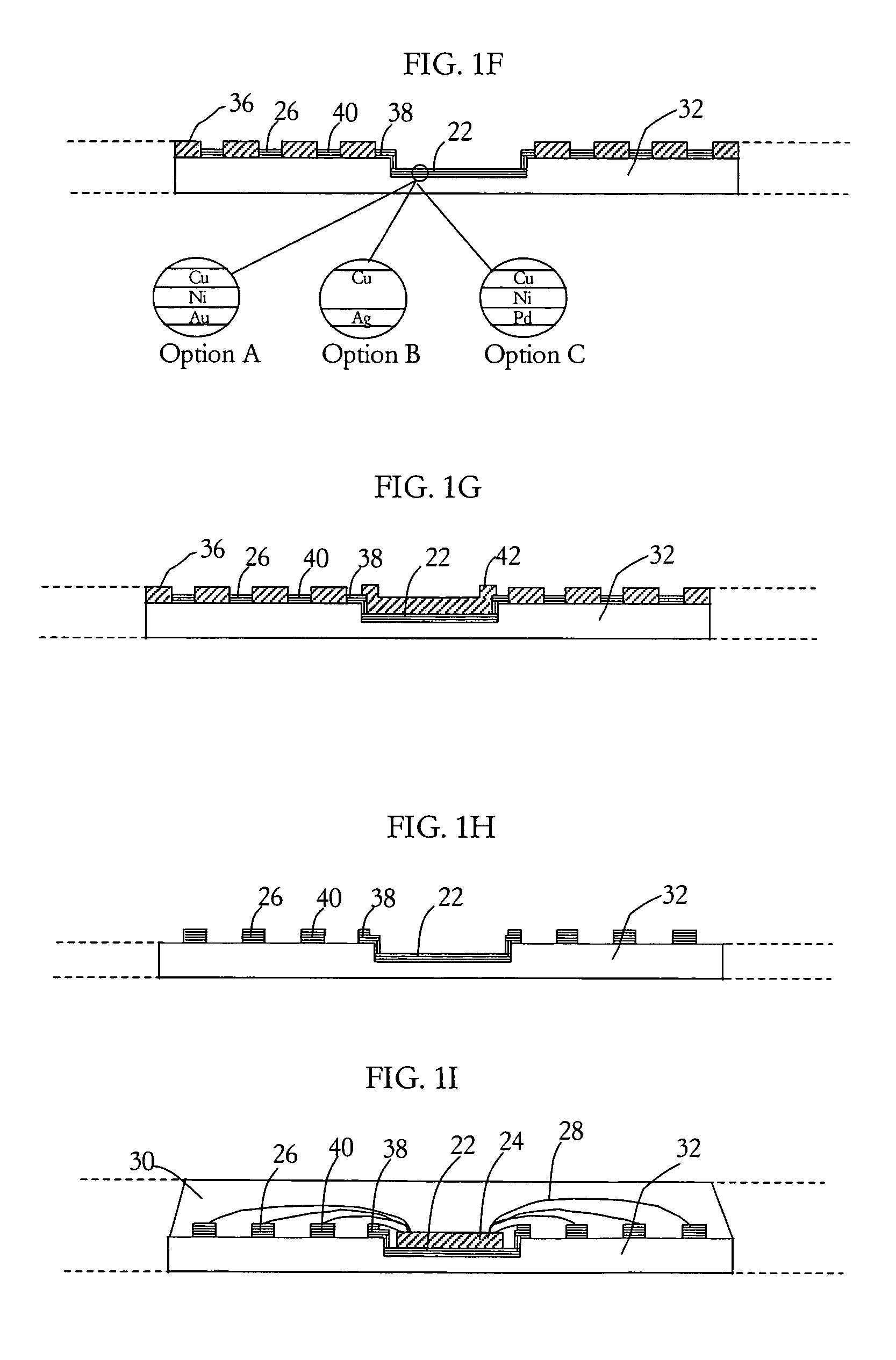
[0016]Reference is first made to FIG. 1L, to describe a Leadless Plastic Chip Carrier (LPCC) indicated generally by the numeral 20. The leadless plastic chip carrier 20 includes a die attach pad 22 and a semiconductor die 24 mounted on the die attach pad 22. A plurality of contact pads 26 circumscribe the die attach pad 22 and a plurality of wire bonds 28 connect the semiconductor die 24 and various ones of the contact pads 26. An overmold 30 covers the semiconductor die 24 and the contact pads 26, wherein the die attach pad 22 is offset from the contact pads 26 such that the die attach pad 22 protrudes from the molding compound 30.

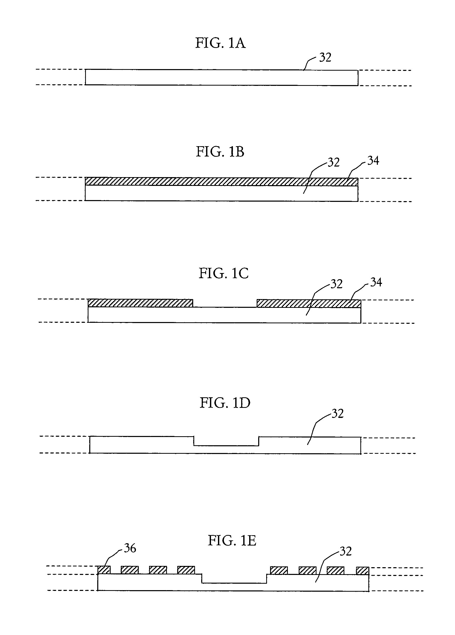
[0017]A process for fabricating the LPCC 20 will now be better described with reference to FIGS. 1A to 1L, which show processing steps for fabricating the LPCC 20 according to an embodiment of the present invention. Referring to FIG. 1A, an elevation view is provided of a Cu (copper) panel substrate which forms the raw material of the leadframe strip 32. ...


PUM


Abstract

A leadless plastic chip carrier is fabricated by selectively etching a leadframe strip to reduce a thickness of the strip at a portion thereof. Selectively masking the surface of the leadframe strip using a mask, follows selectively etching, to provide exposed areas of the surface at the portion and contact pad areas on leadframe the strip. At least one layer of metal is deposited on the exposed areas to define a die attach pad on the portion of the leadframe strip with reduced thickness and to define contact pads on the surface of the strip. At least one semiconductor die is mounted to the die attach pad, followed by wire bonding the at least one semiconductor die to ones of the contact pads. The at least one semiconductor die, the wire bonds, and the contact pads are covered with an overmold material and the leadframe strip is etched to thereby remove the leadframe strip. The leadless plastic chip carrier is singulated from the leadframe strip.

Description

FIELD OF THE INVENTION[0001]The present invention relates in general to integrated circuit packaging, and more particularly to a process for fabricating a leadless plastic chip carrier with a unique, low profile die attach pad.BACKGROUND OF THE INVENTION[0002]According to well known prior art IC (integrated circuit) packaging methodologies, semiconductor dice are singulated and mounted using epoxy or other conventional means onto respective die attach pads (attach paddles) of a leadframe strip. Traditional QFP (Quad Flat Pack) packages incorporate inner leads which function as lands for wire bonding the semiconductor die bond pads. These inner leads typically require mold locking features to ensure proper positioning of the leadframe strip during subsequent molding to encapsulate the package. The inner leads terminate in outer leads that are bent down to contact a mother board, thereby limiting the packaging density of such prior art devices.[0003]In order to overcome these and othe...

Claims


Application Information

Patent Timeline
Patent Type & Authority Patents(United States)
IPC IPC(8): H01L23/06
CPCH01L21/4832H01L21/6835H01L2224/45124H01L2224/45144H01L2924/3011H01L2924/15311H01L2924/01079H01L23/49575H01L2224/48091H01L2224/85001H01L2924/01046H01L2924/01078H01L2924/00014H01L2924/00H01L2224/49433H01L2924/181H01L2924/00012
Inventor KIRLOSKAR, MOHANFAN, CHUN HOTSANG, KWOK CHEUNGKWAN, KIN PUI
Owner UTAC HEADQUARTERS PTE LTD
Why Eureka
Try Eureka