MEMS element, GLV device, and laser display

a laser display and element technology, applied in the field of mems element, glv device, laser display, can solve the problems of etching selectivity ratio and film damage, and achieve the effect of not being damaged

Inactive Publication Date: 2006-03-21
SONY CORP
View PDF4 Cites 67 Cited by
  • Summary
  • Abstract
  • Description
  • Claims
  • Application Information

AI Technical Summary

Benefits of technology

[0037]It is an object of the present invention to provide an MEMS element comprising a membrane having such a constitution as not to be damaged at the time of removing a sacrificing layer by etching in using silicon, such as polysilicon and amorphous silicon, for constituting the sacrificing layer, a GLV device comprised of such MEMS elements, and a laser display comprising such a GLV device.
[0047]The bridge member according to the present invention does not necessarily have the two-layer structure of the SiO2 film and the SiN film. In order to facilitate the control of the elastic force of the bridge member, the bridge member may have a three-layer structure in which another layer, for example, an SiO2 film, is intermediately provided between the metallic film constituting the membrane-side electrode and the SiN film. With the SiO2 film provided intermediately between an Al film and the SiN film, the adhesive force between the SiN film and the Al film is enhanced, and, further, the generation of electrical problems, such as generation of an interface state, can be restrained.
[0065]According to the present invention, by providing the bridge member with a multilayer structure comprising at least two layers including a metal oxide film, such as a silicon oxide film, oppositely to the substrate-side electrode and providing a membrane-side electrode thereon, the film thickness distribution of the membranes due to the etching from the back side of the membranes can be restrained at a minimum at the time of removing the silicon-based sacrificing layer in the fabrication of the MEMS elements.
[0066]By using the MEMS element according to the present invention as a light modulation element, it is possible to enhance light reflectance, enhance light utilization efficiency, enhance the strength of the driver, and enhance the uniformity of driving. By this, in addition, it is possible to enhance the reliability of the MEMS elements and to enlarge the production margins in the fabrication process.
[0067]Further, by composing the GLV device of the MEMS elements according to the present invention, it is possible to realize a GLV device having a high light utilization efficiency and a long useful life. Besides, by incorporating such a GLV device in a laser display, it is possible to realize a laser display having a high light utilization efficiency.

Problems solved by technology

However, it was found that the SiN film is damaged due to the low etching selectivity ratio, as described above.

Method used


Image

  • MEMS element, GLV device, and laser display
  • MEMS element, GLV device, and laser display
  • MEMS element, GLV device, and laser display

Examples


Embodiment Construction

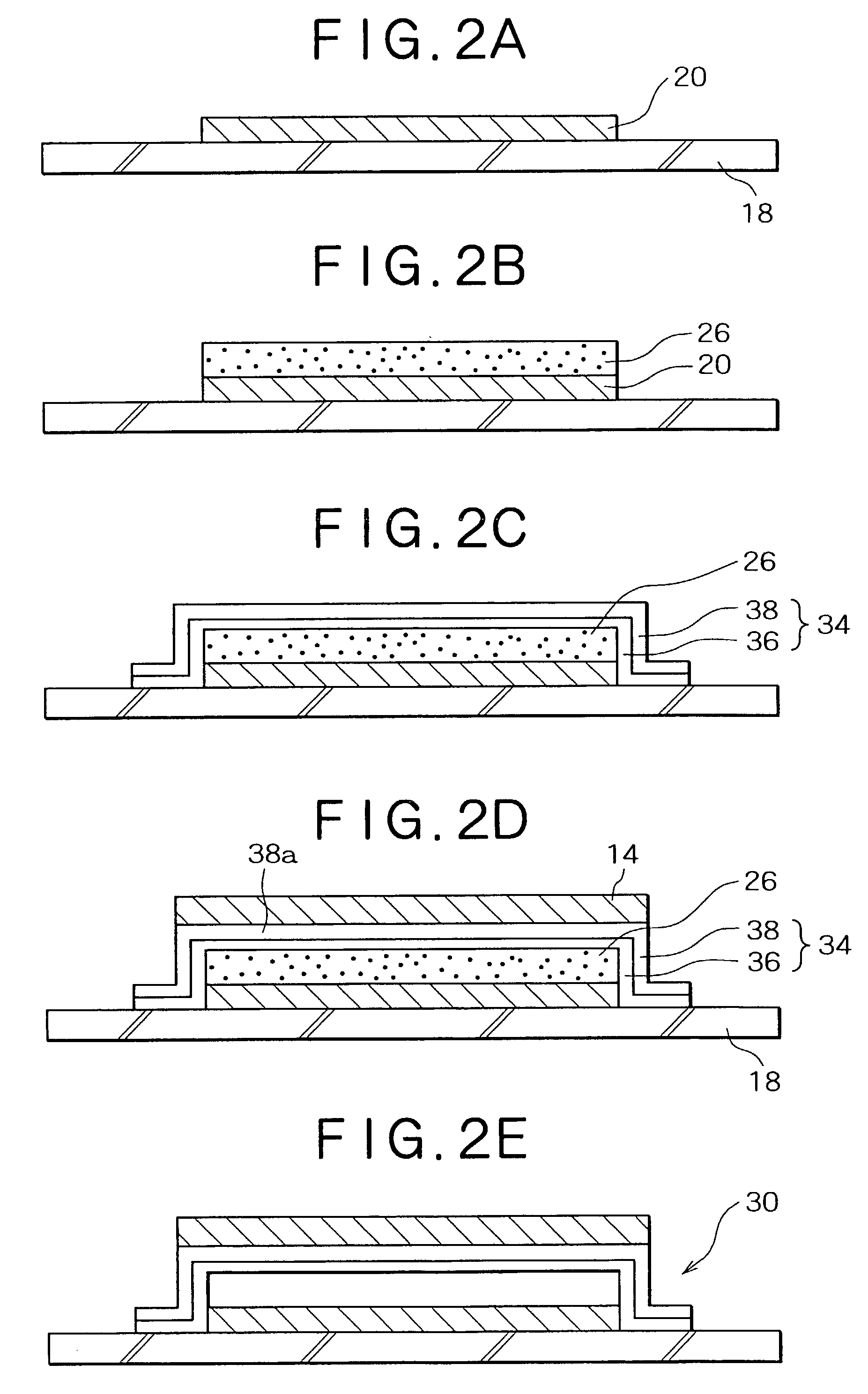
[0077]A mode for carrying out the present invention will be described below concretely and in detail based on embodiments, referring to the accompanying drawings. The film forming method, compositions of layers, film thickness, process conditions and the like shown in the following embodiments are merely an exemplification for easy understanding of the present invention, and the invention is not limited to or by the exemplification.

EMBODIMENT OF MEMS ELEMENT

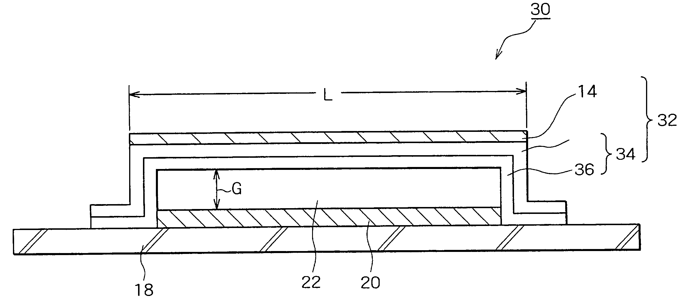
[0078]The present embodiment is one example of embodying the MEMS element according to the present invention, and FIG. 1 is a sectional view showing the constitution of the MEMS element according to the embodiment.

[0079]The MEMS element 30 according to this embodiment is constituted as a light modulation element for constituting a GLV device, and it has the same constitution as the conventional MOEMS 12 except for the difference in the structure of a bridge member 34 of a membrane 32.

[0080]The gap G of a void layer 22 is, for exa...


PUM


Abstract

A MEMS element is constituted as a light modulation element for constituting a GLV device, and it has the same constitution as a conventional MEMS element except for differing in the structure of a bridge member of a membrane. The membrane comprises SiN film of, for example, 100 nm in thickness laminated thereon, and a combined light reflective film and membrane-side electrode composed of an Al film of 100 nm in thickness provided on the bridge member. The SiO2 film may be a SiO2 film formed by thermal oxidation of a sacrificing layer formed of polysilicon or may be a SiO2 film formed by a CVD method or a PVD method.

Description

BACKGROUND OF THE INVENTION[0001]The present invention relates to an MEMS element, a GLV device, and a laser display. More particularly, the invention relates to an MEMS element having such a structure as not to be susceptible to damage at the time of removing a sacrificing layer, particularly an MEMS element having a high light reflectance optimum as a light modulation element, a GLV device comprising the MEMS elements, and a laser display comprising the GLV device.[0002]Attendant on the progress of microtechnology, attention has been paid to the so-called micromachine (MEMS: Micro Electro-Mechanical System) element (hereinafter referred to as MEMS element).[0003]The MEMS element is formed as a microstructure on a substrate, such as a silicon substrate, a glass substrate, and the like, in which a driver for outputting a mechanical driving force and a semiconductor integrated circuit or the like for controlling the driving of the driver are coupled electrically and mechanically. A b...

Claims


Application Information

Patent Timeline
Patent Type & Authority Patents(United States)
IPC IPC(8): G02B26/00B81B7/02G02B26/08H01S3/10
CPCG02B26/0841G02B26/0808
Inventor IKEDA, KOICHISHIMADA, TAKASHI
Owner SONY CORP
Why Eureka
Try Eureka