Laser-based irradiation apparatus and methods for monitoring the dose-rate response of semiconductor devices

a laser-based irradiation and device technology, applied in individual semiconductor device testing, instruments, electroluminescent light sources, etc., can solve the problems of devices becoming even more sensitive to transient ionizing radiation effects, known deleterious effects on semiconductor devices and circuits, and degrading the performance of electronic devices

Inactive Publication Date: 2006-03-28
NAT TECH & ENG SOLUTIONS OF SANDIA LLC
View PDF3 Cites 27 Cited by
  • Summary
  • Abstract
  • Description
  • Claims
  • Application Information

AI Technical Summary

Benefits of technology

[0012]The present invention is directed to a focused laser irradiation apparatus for imaging the dose-rate response of a semiconductor device, comprising a laser providing a beam of laser light of a wavelength, means for focusing the laser beam to a focal spot on the surface of the semiconductor device, means for scanning the focused laser beam at a plurality of spatial locations on the surface of the semiconductor device, means for pulsing the focused laser beam to provide a laser light pulse having a pulse width at each of the spatial locations on the surface of the semiconductor device to provide a charge collection signal at each of the spatial locations, and means for processing the charge

Problems solved by technology

The effects of harsh radiation environments, such as are encountered in space, military, or nuclear power applications, are known to have deleterious effects on semiconductor devices and circuits.
Recent studies have further shown that prolonged exposures to even low levels of radiation can degrade the performance of electronic devices.
Compounding these effects, the continued reduction in feature size of modern commercial integrated circuits (ICs) can result in these devices becoming even more sensitive to transient ionizing radiation effects.
The generation and collection of this unintended electrical charge within the circuit can alter the performance and reliability of specific circuit structures within the device.
Historically, the greatest obstacle to monitoring the radiation response of electronic devices used in long-lived electrical systems has been the destructive nature of most traditional radiation testing techniques.
Moreover, existing radiation test techniques typically do not provide sufficient spatial information about the exact location of the radiation response changes within a die to permit targeted application of modern failure analysis techniques, such as are applied during the production

Method used


Image

  • Laser-based irradiation apparatus and methods for monitoring the dose-rate response of semiconductor devices
  • Laser-based irradiation apparatus and methods for monitoring the dose-rate response of semiconductor devices
  • Laser-based irradiation apparatus and methods for monitoring the dose-rate response of semiconductor devices

Examples


Embodiment Construction

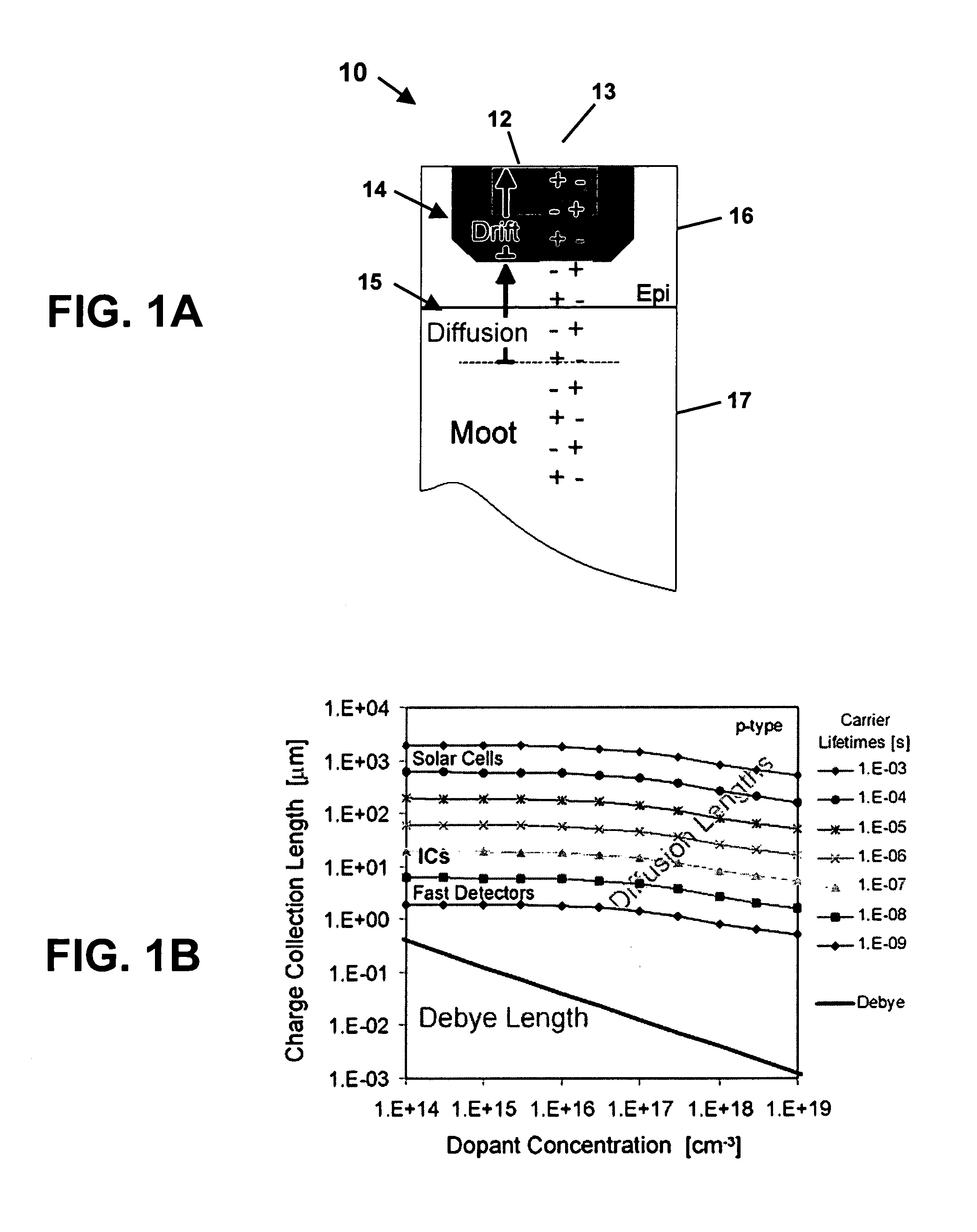
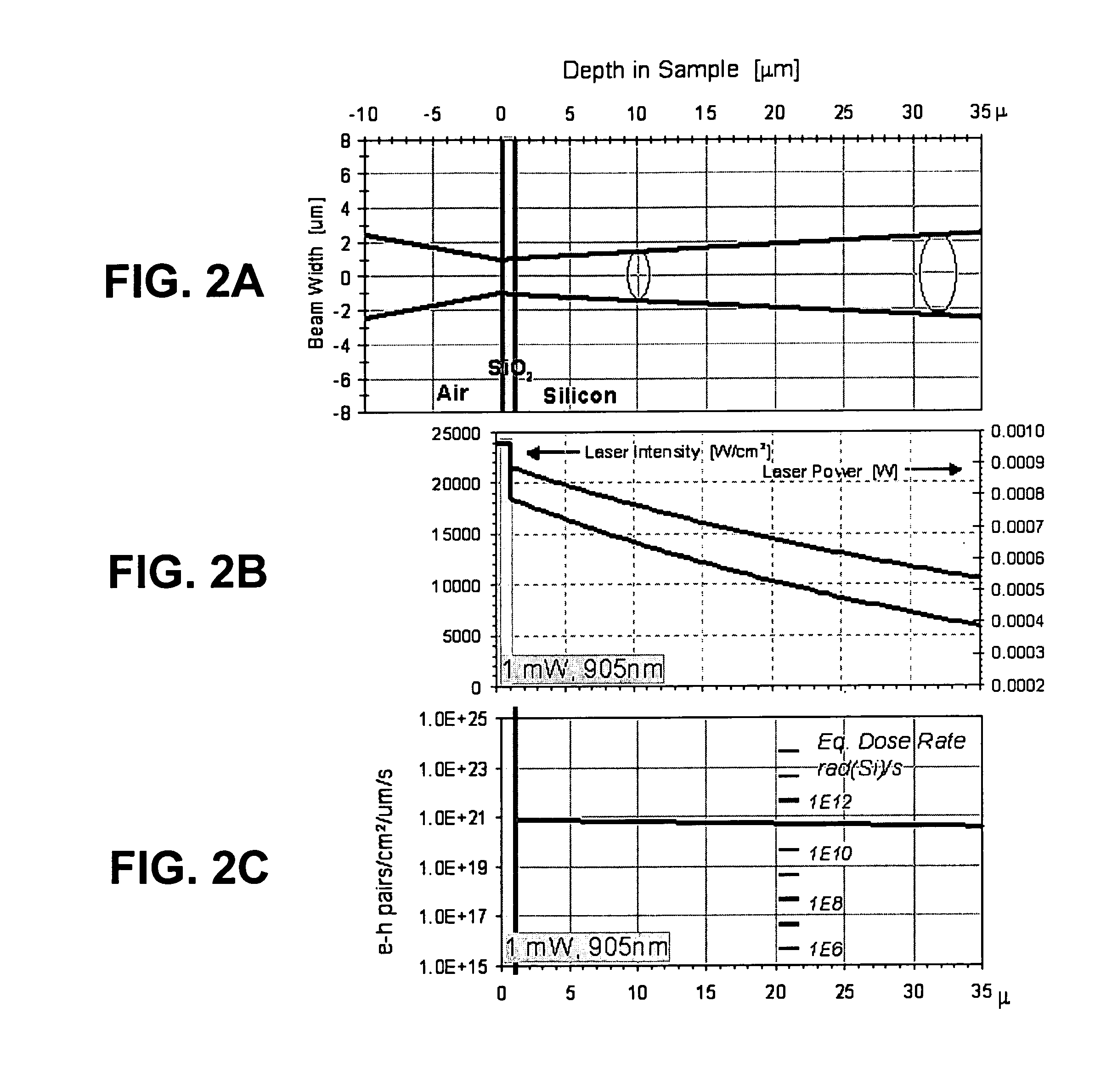
[0027]For use in radiation effects testing, infrared light can replicate the charge collection effects of far more penetrating ionizing radiations. This replication is possible, since only the charge produced in the first few tens of microns of silicon contributes to charge collection within the electrically active regions in most modern semiconductor devices. Electron-hole pairs produced deeper in the device by more penetrating radiations, such as x-rays, gamma-rays, or energetic electrons or ions, recombine before collection into circuit structures near the device surface, and therefore do not affect the normal electrical operation of the device. Consequently, the charge generated in the electrically active regions of the device by the deposition of the laser energy can be made comparable to the total charge generated in those same regions by far more penetrating radiation.

[0028]As shown in FIG. 1A, photocurrent collected in the electrically active region (e.g., a p-n junction) 12...


PUM


Abstract

A scanned, pulsed, focused laser irradiation apparatus can measure and image the photocurrent collection resulting from a dose-rate equivalent exposure to infrared laser light across an entire silicon die. Comparisons of dose-rate response images or time-delay images from before, during, and after accelerated aging of a device, or from periodic sampling of devices from fielded operational systems allows precise identification of those specific age-affected circuit structures within a device that merit further quantitative analysis with targeted materials or electrical testing techniques. Another embodiment of the invention comprises a broad-beam, dose rate-equivalent exposure apparatus. The broad-beam laser irradiation apparatus can determine if aging has affected the device's overall functionality. This embodiment can be combined with the synchronized introduction of external electrical transients into a device under test to simulate the electrical effects of the surrounding circuitry's response to a radiation exposure.

Description

STATEMENT OF GOVERNMENT INTEREST[0001]This invention was made with Government support under contract no. DE-AC04-94AL85000 awarded by the U.S. Department of Energy to Sandia Corporation. The Government has certain rights in the invention.FIELD OF THE INVENTION[0002]The present invention relates to ionizing radiation effects in semiconductor devices and, in particular, to a laser-based irradiation apparatus and methods to measure and image electrical charge collection in semiconductor devices in response to pulsed infrared laser irradiation.BACKGROUND OF THE INVENTION[0003]The effects of harsh radiation environments, such as are encountered in space, military, or nuclear power applications, are known to have deleterious effects on semiconductor devices and circuits. Recent studies have further shown that prolonged exposures to even low levels of radiation can degrade the performance of electronic devices. Compounding these effects, the continued reduction in feature size of modern co...

Claims


Application Information

Patent Timeline
IPC IPC(8): G01R31/28
CPCG01R31/2881G01R31/311
Inventor HORN, KEVIN M.
Owner NAT TECH & ENG SOLUTIONS OF SANDIA LLC
Why Eureka
Try Eureka