Surface emitting semiconductor laser and method of fabricating the same

a semiconductor laser and surface-emitting technology, applied in the direction of lasers, semiconductor lasers, coatings, etc., can solve the problems of reducing the lifetime of the laser device, reducing the strength of the laser, and reducing the efficiency of the laser devi

Inactive Publication Date: 2006-03-28
FUJIFILM BUSINESS INNOVATION CORP
View PDF8 Cites 20 Cited by
  • Summary
  • Abstract
  • Description
  • Claims
  • Application Information

AI Technical Summary

Benefits of technology

[0008]More specifically, the present invention provides a surface emitting semiconductor laser comprising: a substrate; a first mirror that is formed on the substrate and includes semiconductor layers of a first conduction type; a second mirror that includes semiconductor layers of a second conduction type; an active region disposed between the first and second mirrors; a current confinement layer that is disposed between the first and second mirrors and includes a selectively oxidized region; and an inorganic insulation film, a mesa structure including at least the second mirror and the current confinement layer, the inorganic insulation film covering at least a side surface of the mesa structure and having an internal stress equal to or less than 1.5×10⁹ dyne/cm2.
[0009]According to another aspect of the invention, there is provided a surface emitting semiconductor laser comprising: a substrat

Problems solved by technology

This prevents the mesa structure from caving in and lengthens the lifetime of the laser device.
However, the inventors found that the following problems still remain in the device structure disclosed in the above-mentioned application.
In case where a magnitude of internal stress greater than a certain level is e

Method used


Image

  • Surface emitting semiconductor laser and method of fabricating the same
  • Surface emitting semiconductor laser and method of fabricating the same
  • Surface emitting semiconductor laser and method of fabricating the same

Examples


first embodiment

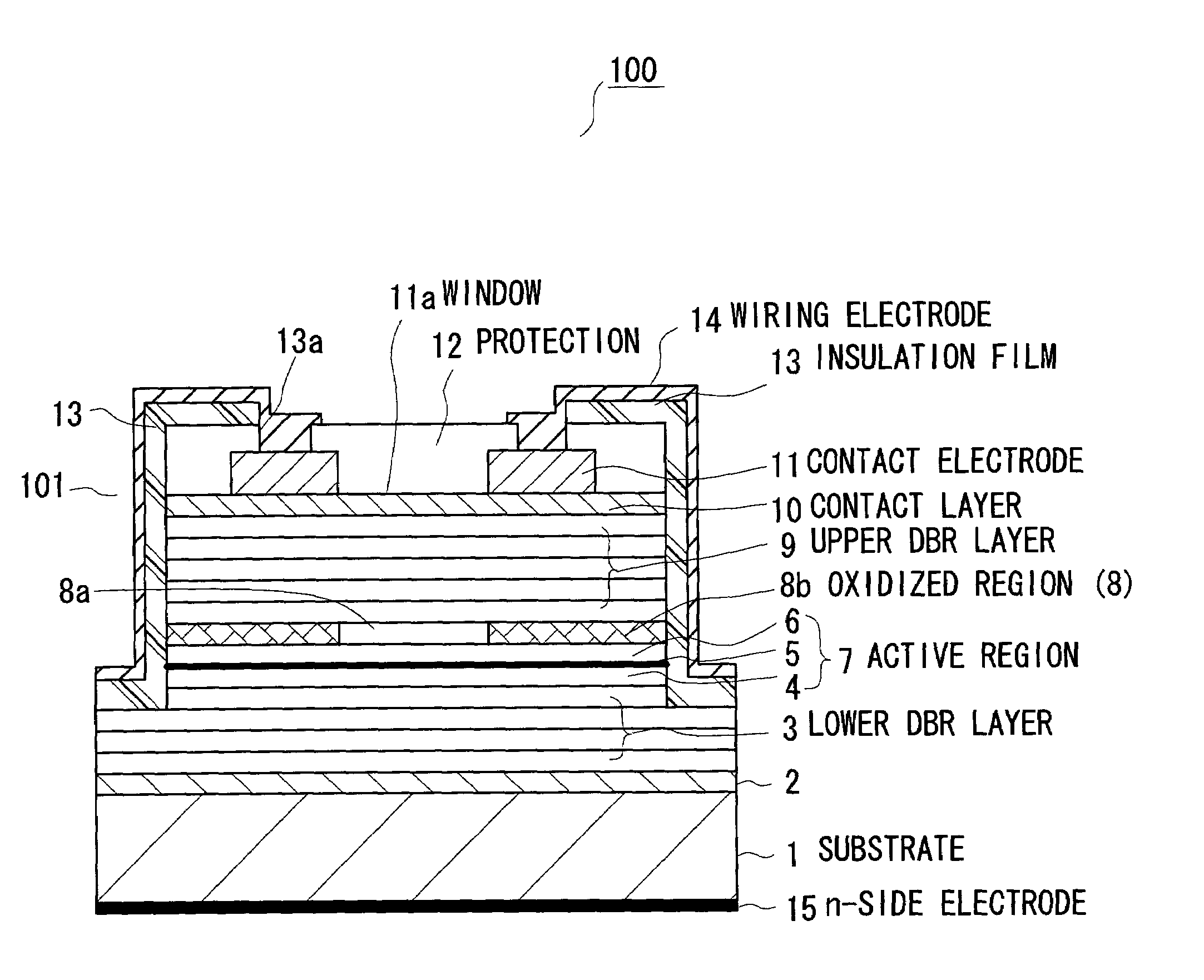
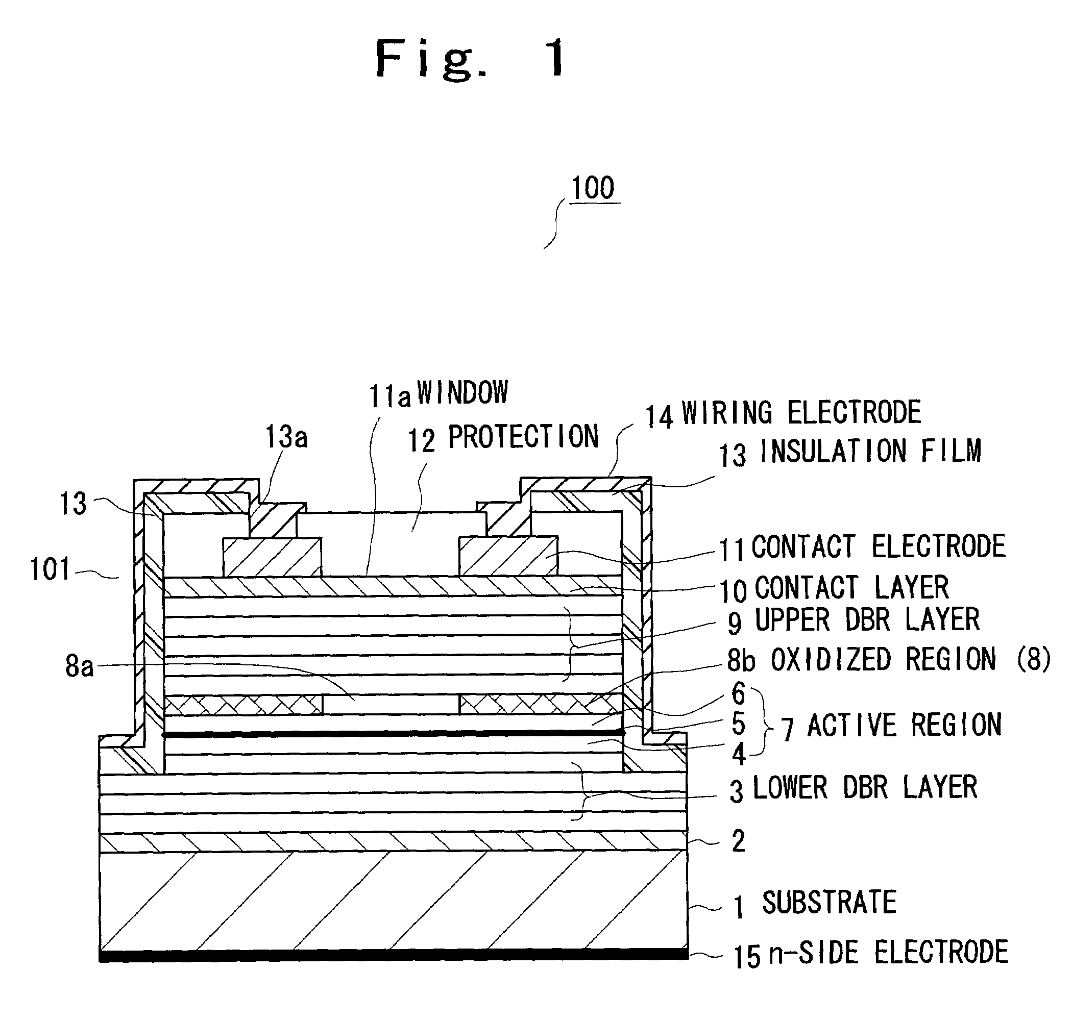
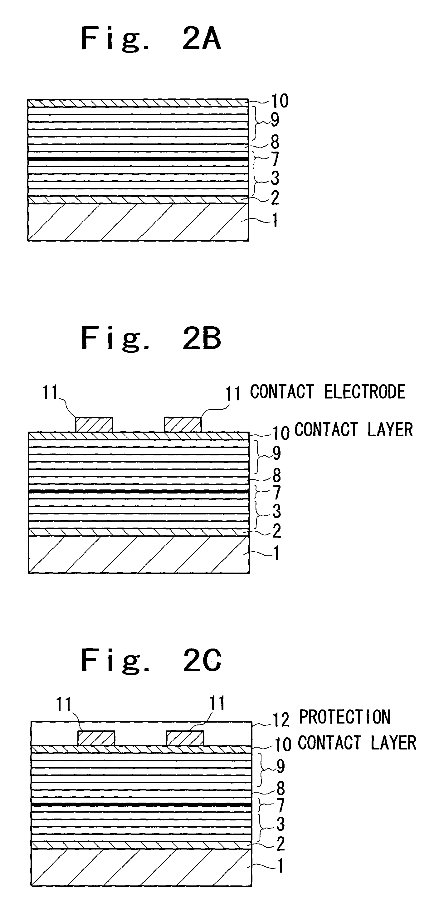
[0019]FIG. 1 is a cross-sectional view of a surface emitting semiconductor laser according to an embodiment of the present invention. Referring to FIG. 1, a surface emitting semiconductor laser 100 has a laser device part 101 having a mesa structure of a cylindrical shape. The mesa structure may be called a post structure or pillar structure. It should be noted that a protection or passivation film with which the mesa structure 101 is coated and a bonding pad extending from a metal contact layer are omitted from FIG. 1 for the sake of simplicity.

[0020]The laser 100 has an n-type GaAs substrate 1, an n-type GaAs buffer layer 2 formed on the GaAs substrate 1, an n-type lower DBR (Distributed Bragg Reflector) layer 3, and an active region 7 formed on the lower DBR layer 3. The active region 7 is a laminate of an undoped lower spacer layer 4, an undoped quantum well layer 5, and an undoped upper spacer layer 6. A current confinement layer 8, which controls current, is provided on the ac...

second embodiment

[0051]A description will now be given of a second embodiment of the present invention. A surface emitting semiconductor laser according to the present embodiment differs from the first embodiment in that the second embodiment has a different structure of the interlayer insulation film and the interlayer insulation film remains on the outgoing light window protection film. Further, the silicon nitride film as the mask is used in the depositing process of the mask for forming the mesa (the process of FIG. 2E) in the first embodiment, while the silicon oxynitride film for the mask is deposited in the second embodiment. The other structures and processes of the second embodiment are the same as those of the first embodiment.

[0052]In the step of FIG. 2I according to the second embodiment of the present invention, the interlayer insulation film 13 is formed in a region including the mesa and the mesa bottom. For example, the interlayer insulation film 13 may be deposited to 800 nm by PCVD...

third embodiment

[0057]A description will now be given of a third embodiment of the present invention. A surface emitting semiconductor laser according to the third embodiment of the invention differs from that of the first embodiment in the structure of the interlayer insulation film.

[0058]In the step of FIG. 2I according to the third embodiment of the present invention, multiple silicon nitride films having tensile stress and compressive stress are laminated to form the interlayer insulation film.

[0059]A silicon nitride film having tensile stress is deposited to 400 nm under the following condition:

[0060]

ConditionQuantityUnitmonosilane35ccmammonia240ccmhydrogen0ccmnitrogen0ccmRF power100Wsubstrate temperature250° C.pressure26.6Pa

[0061]The tensile stress of the silicon nitride film thus formed is 3×10⁹ dyne / cm2.

[0062]A silicon nitride film having compressive stress is deposited to 400 nm under the following condition:

[0063]

ConditionQuantityUnitmonosilane35ccmammonia105ccmhydrogen280ccmnitrogen70ccm...


PUM

PropertyMeasurementUnit
Fractionaaaaaaaaaa
Fractionaaaaaaaaaa
Pressureaaaaaaaaaa

Abstract

A surface emitting semiconductor laser includes a substrate, a first mirror that is formed on the substrate and includes semiconductor layers of a first conduction type, a second mirror that includes semiconductor layers of a second conduction type, an active region disposed between the first and second mirrors, a current confinement layer that is disposed between the first and second mirrors and includes a selectively oxidized region, and an inorganic insulation film. A mesa structure includes at least the second mirror and the current confinement layer. The inorganic insulation film covers at least a side surface of the mesa structure and having an internal stress equal to or less than 1.5×10⁹ dyne/cm2.

Description

BACKGROUND OF THE INVENTION[0001]1. Field of the Invention[0002]The present invention relates to a surface emitting semiconductor laser and a method of fabricating the same, and more particularly, to a selective oxidization type surface emitting semiconductor laser and a method of fabricating the same.[0003]2. Description of the Related Art[0004]Recently, there has been an increased demand for a surface emitting semiconductor laser that has advantages of easy arrangement of a two-dimensional array of sources and low threshold current and low power consumption. These advantages are attractive in the technical fields of optical communications and optical recording. Such a surface emitting semiconductor laser is also called a vertical-cavity surface-emitting laser (VCSEL).[0005]The inventors of the present invention have proposed an improved surface emitting semiconductor laser that has a lengthened lifetime and even output power in Japanese Laid-Open Patent Application Publication No....

Claims


Application Information

Patent Timeline
IPC IPC(8): H01S5/00C23C16/42H01L21/318H01S3/13H01S5/042H01S5/18H01S5/183H01S5/30H01S5/343
CPCB82Y20/00H01S5/18311H01S5/0425H01S5/0021H01S5/0282H01S2301/176H01S5/3201H01S5/3432H01S5/04254
Inventor YAMAMOTO, MASATERUSAKURAI, JUN
Owner FUJIFILM BUSINESS INNOVATION CORP
Why Eureka
Try Eureka