High speed photodiode with a barrier layer for blocking or eliminating slow photonic carriers and method for forming same

a photonic carrier and barrier layer technology, applied in the field of photodiodes, can solve the problems of difficult to distinguish one bit from the other, inability to transfer information in a long tail, and weak electric field which is induced deep in the semiconductor, so as to reduce the lifetime of the carrier

Inactive Publication Date: 2006-04-04
GLOBALFOUNDRIES U S INC
View PDF13 Cites 3 Cited by
  • Summary
  • Abstract
  • Description
  • Claims
  • Application Information

AI Technical Summary

Benefits of technology

[0025]The present invention provides a method (and structure) in which a buried barrier is combined with a photodetector to block or eliminate the slow carriers. The buried barrier layer does not form an etalon, and may serve as a diffusive mirror.
[0030]In a third embodiment of the present invention, a photodiode such as a Si LTD, includes alternating lateral n+ and p+ fingers built into lightly doped n-type or p-type absorption layer, is formed over a buried “bubble” layer that is embedded in the substrate. The bubble layer is for blocking and eliminating the slow carriers that are generated relatively deep in the substrate.
[0034]Indeed, with regard to the P-N junction embodiment, the mechanism by which the present invention obtains the blocking of the carriers with a P-N junction is completely different from a heavily doped layer for reducing the carriers' lifetime.

Problems solved by technology

A problem arises in that an electric field which is induced deep in the semiconductor is not as strong as that near the surface at the anode and cathode.
However, if the carriers are collected over a long period of time, then instead of a short current pulse, one would obtain a fast rise in the current followed by a slow decay (e.g., a long “tail”), since it takes some time to collect the deep (slow) carriers.
This is a problem in that the “long tail” is unacceptable for transfer of information and the like, especially over an optical fiber.
Otherwise, it would be difficult to distinguish one bit from another if the long tail was present.
This limits the bit rate that can be used with this photodetector.
However, the carriers generated below the deep trenches limit the bandwidth, as described in M. Yang, et al., Proceedings of the 59th DRC, p.
Such tight control is difficult to obtain over a single wafer and from wafer-to-wafer.
The minima should be avoided if possible, but this is difficult to achieve if the photodetector structure layer is thick, since then the minima are very closely spaced.
On the other hand, while it may be possible to make the layer thinner, then there would not be a large absorption volume and the quantum efficiency would suffer (e.g., the amount of photons which are converted into electrons is very poor).
Moreover, the use of SOI has other disadvantages.
For example, the cost of a SOI wafer is currently about five times that of bulk silicon.
The heavily doped layer has a short lifetime for minority carriers, thus increasing the chance of recombination for slow carriers that were formed below the heavily doped layer.
Further, such a heavily doped layer is difficult to manufacture due to dopant diffusion problems.
Indeed, while it is disclosed that the heavily doped layer reduces the carriers lifetime, there is nothing disclosed about the formation of a potential barrier to block the carriers.

Method used


Image

  • High speed photodiode with a barrier layer for blocking or eliminating slow photonic carriers and method for forming same
  • High speed photodiode with a barrier layer for blocking or eliminating slow photonic carriers and method for forming same
  • High speed photodiode with a barrier layer for blocking or eliminating slow photonic carriers and method for forming same

Examples


first embodiment

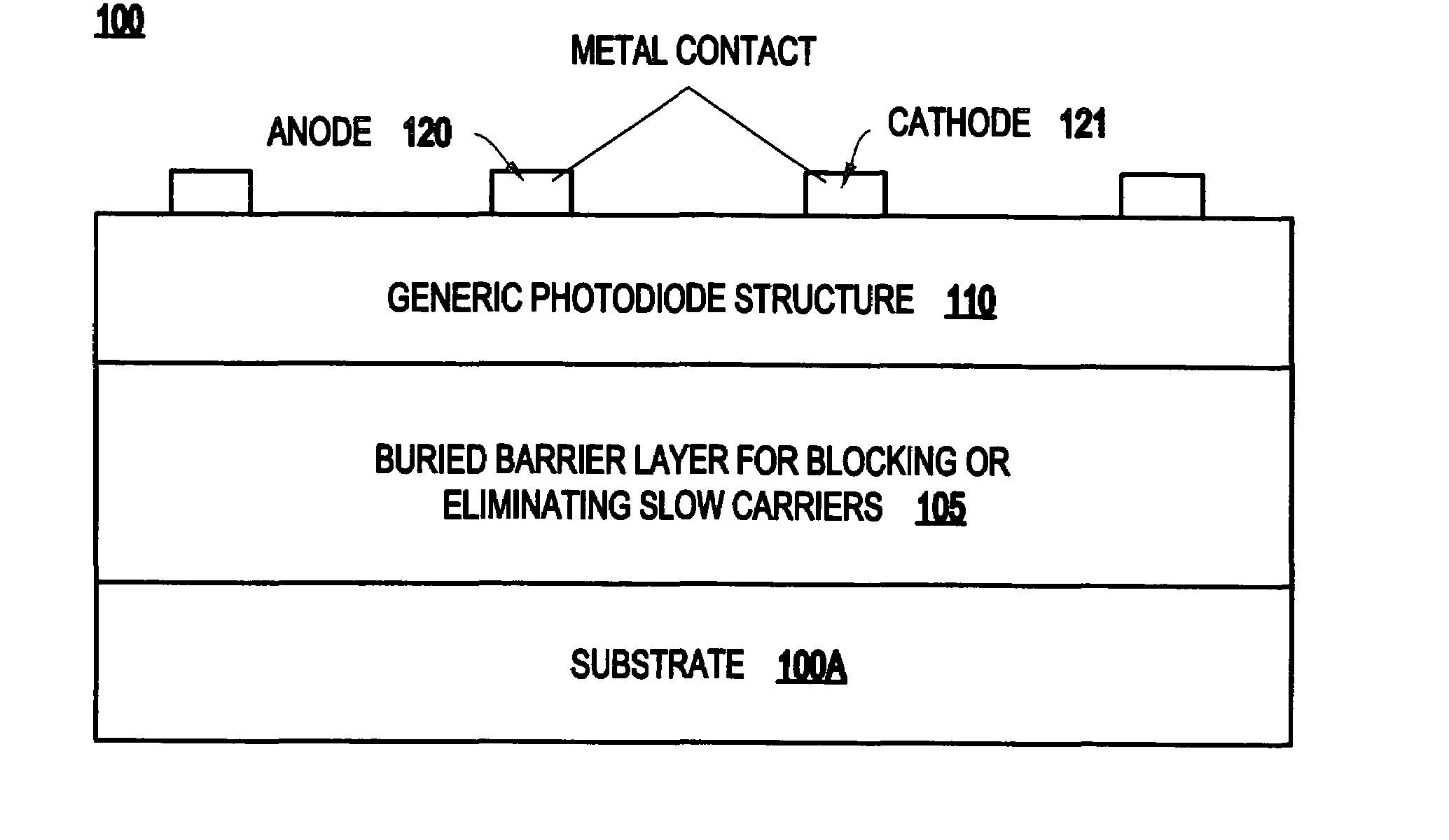
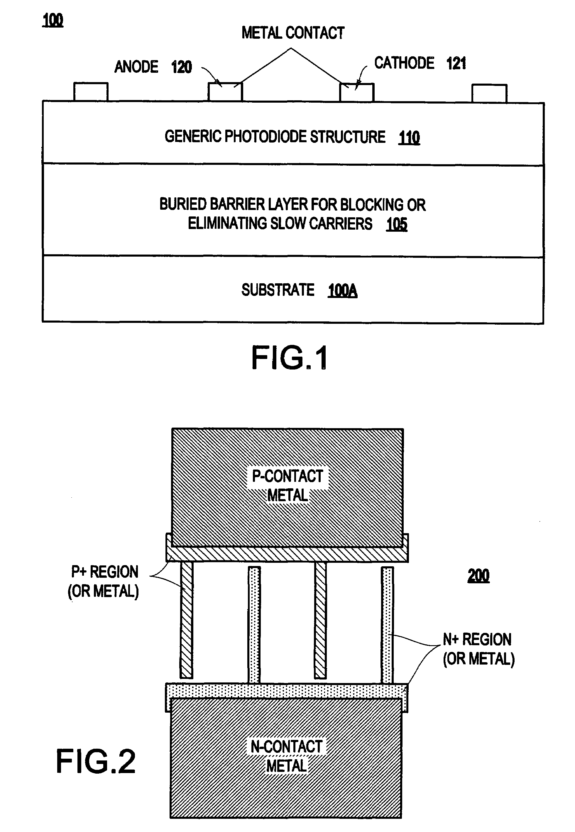
[0083]Thus, the present invention provides a buried PN junction as a barrier layer by forming an implant or the like, and forms an electric barrier to the slow carriers which are absorbed below the PN junction. It is noted that this barrier layer does not necessarily instantly eliminate the slow carriers, but instead blocks the slow carriers from drifting upwardly to the anode and cathode contacts.

[0084]Additionally, in this embodiment, it is noted that the PN junction can be formed with relatively low doping, as opposed to high doping levels as used in the conventional techniques. This will overcome the issues of the processing of the conventional techniques discussed above, including diffusion, etc.

[0085]B. A Bubble Layer as a Barrier

second embodiment

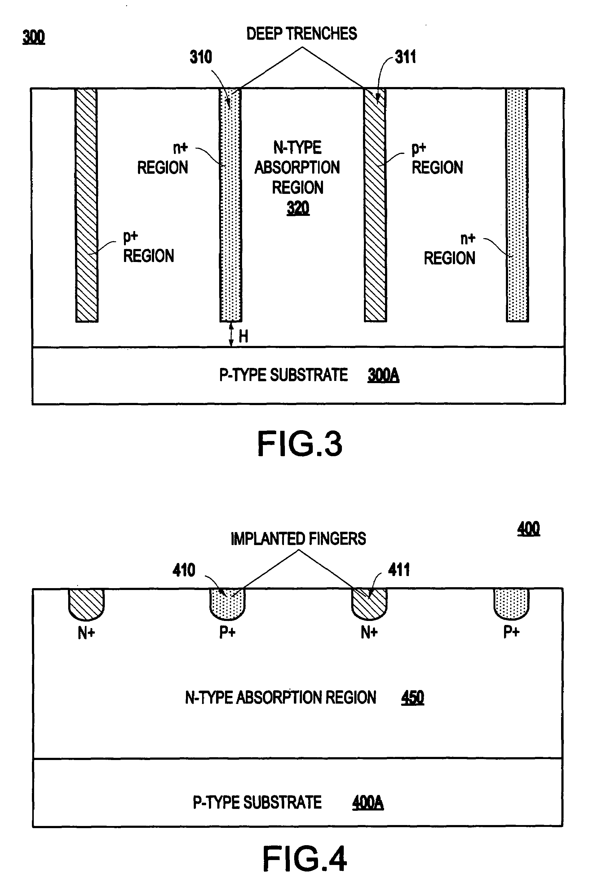
[0086]Turning now to the present invention and FIGS. 9–11, a bubble layer is provided to block and eliminate the slow carriers. The annihilation of the carriers is achieved through very efficient recombination centers introduced by the bubbles and by defects formed between the bubbles.

[0087]FIG. 10 illustrates a structure including a substrate 1000A having a photodiode structure formed over a buried bubble layer 1050. The photodiode structure is a lateral PIN detector with an absorption region 1020, and alternating p+ (1010) and n+ (1011) fingers.

[0088]FIGS. 9 and 11 illustrate similar barrier regions incorporated into lateral trench detector and a metal-semiconductor-metal (MSM) photodetector, respectively.

[0089]Specifically, FIG. 9 illustrates a structure including a substrate 900A having a photodiode structure formed over a buried bubble layer 950. The photodiode structure is a lateral trench PIN detector with an absorption region 920, and alternating n+ (910) and p+ (911) deep t...


PUM


Abstract

A structure (and method for forming the structure) includes a photodetector, a substrate formed under the photodetector, and a barrier layer formed over the substrate. The buried barrier layer preferably includes a single or dual p-n junction, or a bubble layer for blocking or eliminating the slow photon-generated carriers in the region where the drift field is low.

Description

U.S. GOVERNMENT RIGHTS IN THE PATENT[0001]The present invention was at least partially funded under National Institute of Standards and Technology (NIST) Contract No. 70NANB8H4018, and the U.S. Government has at least some rights under any subsequently-issued patent.CROSS-REFERENCE TO RELATED APPLICATIONS[0002]The present application is related to commonly-assigned U.S. patent application Ser. No. 09 / 678,315, filed on Oct. 3, 2000, to Y. H. Kwark et al., entitled “Silicon-on-insulator trench photodiode structure for improved speed and differential isolation” having IBM Docket No. YOR920000052US1, incorporated herein in its entirety.BACKGROUND OF THE INVENTION[0003]1. Field of the Invention[0004]The present invention relates to a semiconductor device, and more particularly to a photodiode, and to a method of forming a buried layer for blocking or eliminating slow photo-generated carriers in a region where the electric field is low.[0005]2. Description of the Related Art[0006]The abso...

Claims


Application Information

Patent Timeline
Patent Type & Authority Patents(United States)
IPC IPC(8): H01L21/00H01L27/146H01L31/0328H01L31/08H01L31/10H01L31/103H01L31/18H04N5/335
CPCH01L31/0232H01L31/1085H01L31/105H01L31/035272H01L31/02327H01L31/10
Inventor COHEN, GUY MOSHEOUYANG, QIQING C.SCHAUB, JEREMY DANIEL
Owner GLOBALFOUNDRIES U S INC
Why Eureka
Try Eureka