Manufacturing method of a semiconductor substrate provided with a through hole electrode

a manufacturing method and semiconductor technology, applied in the direction of cable/conductor manufacture, conductive pattern formation, printed circuit manufacturing, etc., can solve the problems of deterioration of the characteristics of not only the semiconductor substrate itself but also of other electric devices without through hole electrodes, and the process temperature as available is restricted

Active Publication Date: 2006-04-04
FUJIKURA LTD +1
View PDF6 Cites 99 Cited by
  • Summary
  • Abstract
  • Description
  • Claims
  • Application Information

AI Technical Summary

Problems solved by technology

Because of this, there is restriction in process temperatures as available, when thermal treatments are performed after forming a through hole electrode in a semiconductor substrate, depending upon the properties of the conductive material of the through hole electrode, and therefore the selection of devices and wiring patterns which can be formed thereon is limited.
Also, in the case where electric devices are fabricated on the semiconductor substrate provided with a through hole electrode, there are following problems relating to the fabrication process thereof.
If a semiconductor substrate provided with a through hole electrode or a device fabricated thereon is contaminated, the characteristics of not only the semiconductor substrate itself but also of other electric devices having no through hole electrode is deteriorated due to the cross contamination via these equipments.
Moreover, since there are usually formed irregularities of the order of several micrometers on the surface of a through hole electrode, the fabrication process is hampered by the irregularities, depending upon the device to be fabricated.
For example, when a resist is coated on a semiconductor substrate provided with a through hole electrode by means of a spin coater, it becomes difficult to form a resist film in a uniform manner in the vicinity of the irregularities on the surface of the through hole electrode.

Method used


Image

  • Manufacturing method of a semiconductor substrate provided with a through hole electrode
  • Manufacturing method of a semiconductor substrate provided with a through hole electrode
  • Manufacturing method of a semiconductor substrate provided with a through hole electrode

Examples


first embodiment

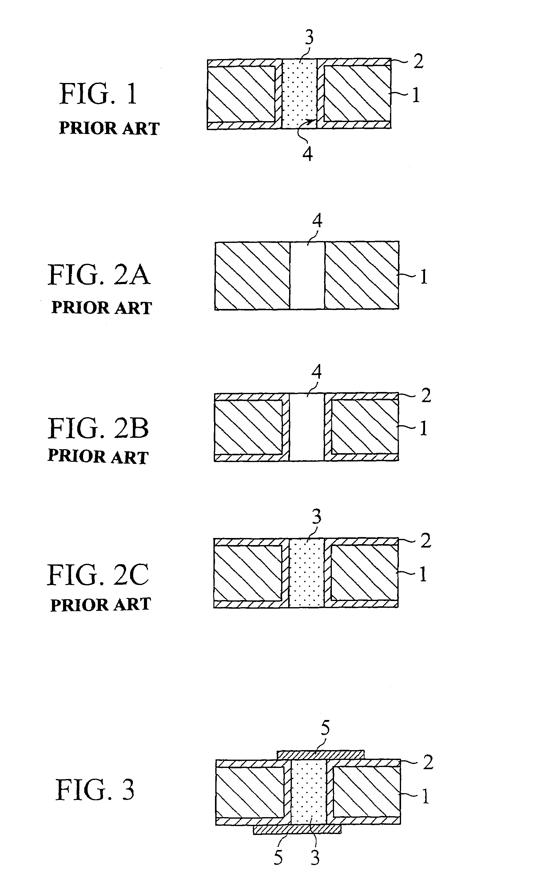
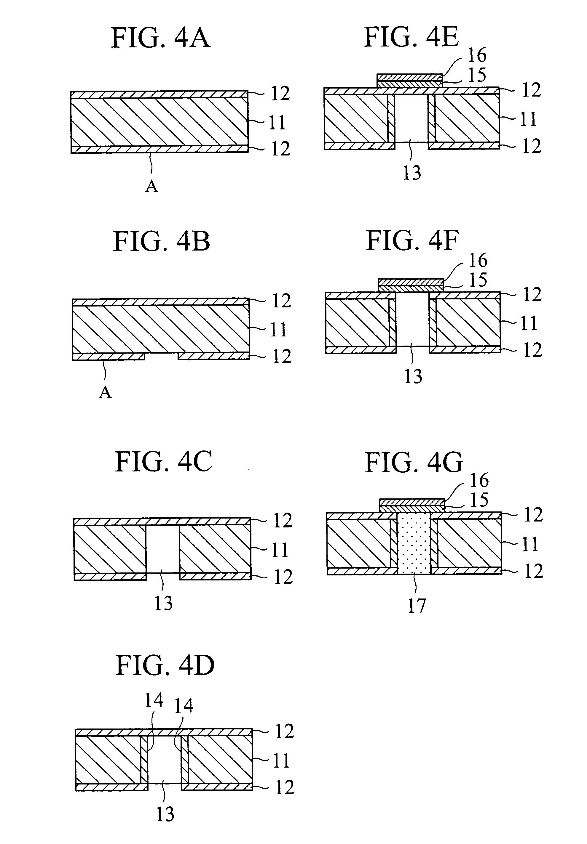
[0033]FIG. 4A through FIG. 4G are cross sectional views showing the method of manufacturing a semiconductor substrate provided with a through hole electrode in accordance with the present invention; the views are arranged in the order of manufacturing. The cross section is normal to the semiconductor substrate and along the longitudinal direction of the through hole electrode. FIG. 5A and FIG. 5B are plan views showing the semiconductor substrate provided with a through hole electrode as seen from the above.

[0034]In this embodiment, an interposer which can be used for 3D stacking is manufactured.

[0035]As illustrated in FIG. 4A, a semiconductor substrate 11 made of a silicon substrate having a thickness of 300 μm or thereabout is prepared, and a first silicon oxide films 12 (acting as insulating layer) having a thickness of 1 μm or the like are formed on both the upper and lower surfaces (principal surfaces) of the substrate 11 (a first insulating layer formation step). In this embod...

second embodiment

[0059]With reference to FIG. 7A to FIG. 7F and FIG. 8A to FIG. 8B, the manufacturing method in accordance with the present invention will be explained.

[0060]In this embodiment, a semiconductor device provided with a through hole electrode is manufactured. Specifically, a through hole electrode is formed through a semiconductor substrate on which a general purpose IC chip for driving and controlling MEMS (Micro Electro Mechanical Systems) or other MEMS devices such as a sensor are provided.

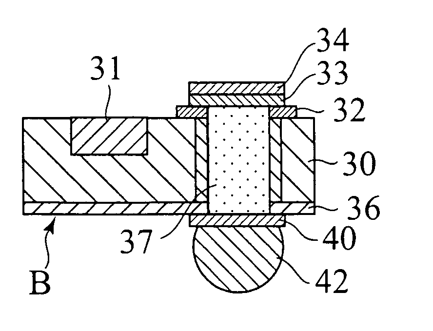
[0061]FIG. 7A through FIG. 7F are cross sectional views of a semiconductor device showing the method of this embodiment and arranged in order of manufacturing. The cross section is normal to the plane of the semiconductor substrate and along the longitudinal direction of the through hole electrode. FIG. 8A and FIG. 8B are plan views showing the semiconductor device provided with a through hole electrode as seen from the above.

[0062]As illustrated in FIG. 7A, a first silicon oxide film 32 having a t...


PUM

PropertyMeasurementUnit
thicknessaaaaaaaaaa
thicknessaaaaaaaaaa
conductiveaaaaaaaaaa

Abstract

A manufacturing method of a semiconductor substrate provided with a through hole electrode is proposed. In accordance with the methods, it is possible to effectively form a through hole electrode in a semiconductor substrate in which a device and a wiring pattern have been already fabricated. This manufacturing method includes the steps of forming a first silicon oxide film 12 on a principal surface of the semiconductor substrate 11, forming a small hole 13 through the semiconductor substrate 11 from the opposite the step to reach to the first silicon oxide film 12, covering the inside of the small hole 13 with the second silicon oxide film 14, forming a first thin metal film 15 and a second thin metal film 16 on the first silicon oxide film 12, partially removing the first silicon oxide film 12 corresponding to the end of the small hole 13, and filling the small hole 13 with the conductive material to form a through hole electrode 17.

Description

CROSS REFERENCE TO RELATED APPLICATIONS[0001]The subject application is related to subject matter disclosed in the Japanese Patent Application No.2002-254858 filed in Aug. 30, 2002 in Japan, to which the subject application claims priority under the Paris Convention and which are incorporated by reference herein.BACKGROUND OF THE INVENTION[0002]1. Field of the Invention[0003]The present invention relates to a manufacturing method of a semiconductor substrate provided with a through hole electrode.[0004]2. Description of the Related Art[0005]Semiconductor substrates provided with a through hole electrode have been used for electrical connections of various types of electronic devices, optical devices and the like, or as an interposer for three-dimensional (3D) stacked devices.[0006]FIG. 1 is a schematic cross section view showing an example of a semiconductor substrate provided with a through hole electrode.[0007]This semiconductor substrate provided with a through hole electrode is ...

Claims


Application Information

Patent Timeline
Patent Type & Authority Patents(United States)
IPC IPC(8): H01L21/302H01L23/52H01L21/3205H01L21/60H01L21/768H01L23/12H01L23/48
CPCH01L21/76898H01L23/481H01L2924/0002Y10T29/49155Y10T29/49156H01L2224/05H01L2224/02372H01L2224/05025H01L2224/0557H01L2224/06181H01L2224/131H01L2224/0401H01L2924/014H01L2224/05552
Inventor YAMAMOTO, SATOSHITAKIZAWA, TAKASHISUEMASU, TATSUOKATASHIRO, MASAHIROMIYAJIMA, HIROSHIMATSUMOTO, KAZUYAISOKAWA, TOSHIHIKO
Owner FUJIKURA LTD
Why Eureka
Try Eureka