Method for forming polycrystalline silicon thin film transistor

a thin film transistor and polycrystalline silicon technology, applied in the direction of semiconductor devices, instruments, electrical equipment, etc., can solve the problems of difficult to realize the driving elements of peripheral circuits, a-si tft cannot meet such an operation speed, and the difficulty of producing all switching elements in the liquid crystal display device, so as to prevent the degradation of electrons and holes

Active Publication Date: 2006-04-11
BOE HYDIS TECH CO LTD
View PDF4 Cites 0 Cited by
  • Summary
  • Abstract
  • Description
  • Claims
  • Application Information

AI Technical Summary

Benefits of technology

[0014]Accordingly, the present invention has been made to solve the above-mentioned problems occurring in the prior art, and an object of the present invention is to provide a method for forming a poly-Si TFT, which can prevent degradation of the mobility of electrons and holes in operation of the TFT while employing the SLS method for development of crystal grains, so that the poly-Si TFT has a uniform TFT characteristic over the entire substrate.

Problems solved by technology

However, an a-Si TFT having an active layer made from amorphous silicon has a very low mobility of about 0.5 cm2 / Vs, which makes it difficult to produce all switching elements in the liquid crystal display device.
In other words, driving elements for peripheral circuits of the liquid crystal display device have to operate at a very high speed, and the a-Si TFT cannot satisfy such an operation speed as required by the driving elements for peripheral circuits.
Therefore, it is actually difficult to realize the driving elements for peripheral circuits by using the a-Si TFT.
However, this method may cause deformation of the glass substrate at a temperature above 600° C., thereby degrading reliability and reducing yield of the products.
Here, the protrusion has many defects because it is formed by the collision between two kinds of crystal grains having different orientations.
Therefore, if a protrusion is formed in a channel area of a poly-Si TFT while the TFT is formed through crystallization of the a-Si layer using the SLS method, the protrusion largely degrades the mobility of electrons and holes when the TFT is operated.
Also, if a protrusion is formed in a drain area of the poly-Si TFT, the current leakage increases.
Therefore, even in a transistor having the same channel length and width, the TFT characteristic shows a large difference between the existence or absence of the protrusion, which becomes a source causing the TFT characteristic of the entire substrate to be non-uniform.

Method used


Image

  • Method for forming polycrystalline silicon thin film transistor
  • Method for forming polycrystalline silicon thin film transistor

Examples


Embodiment Construction

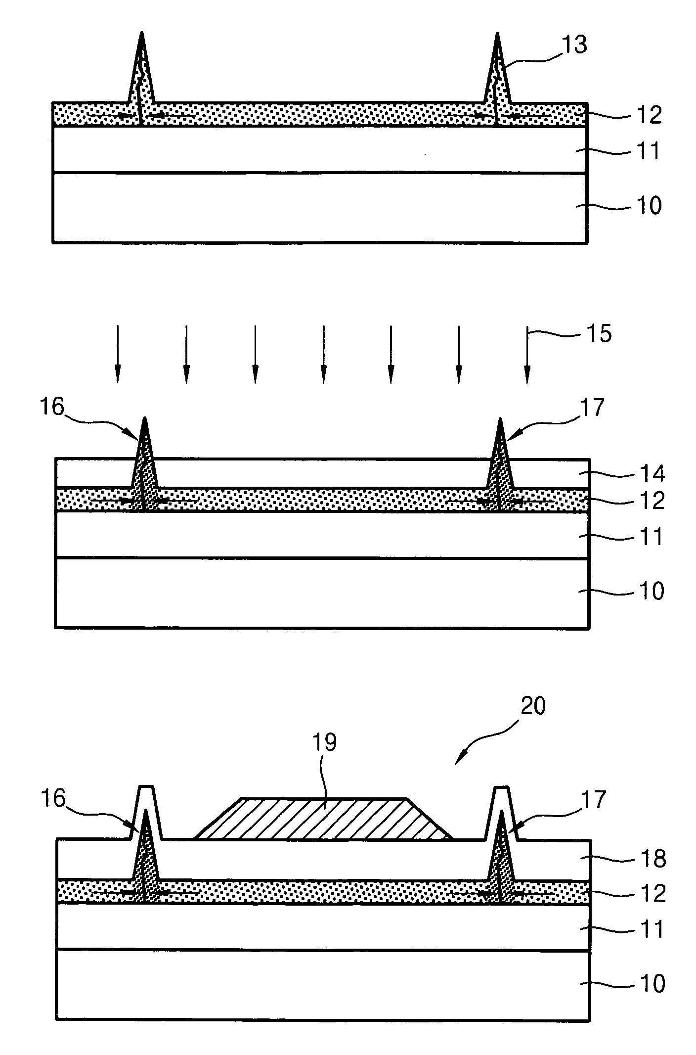
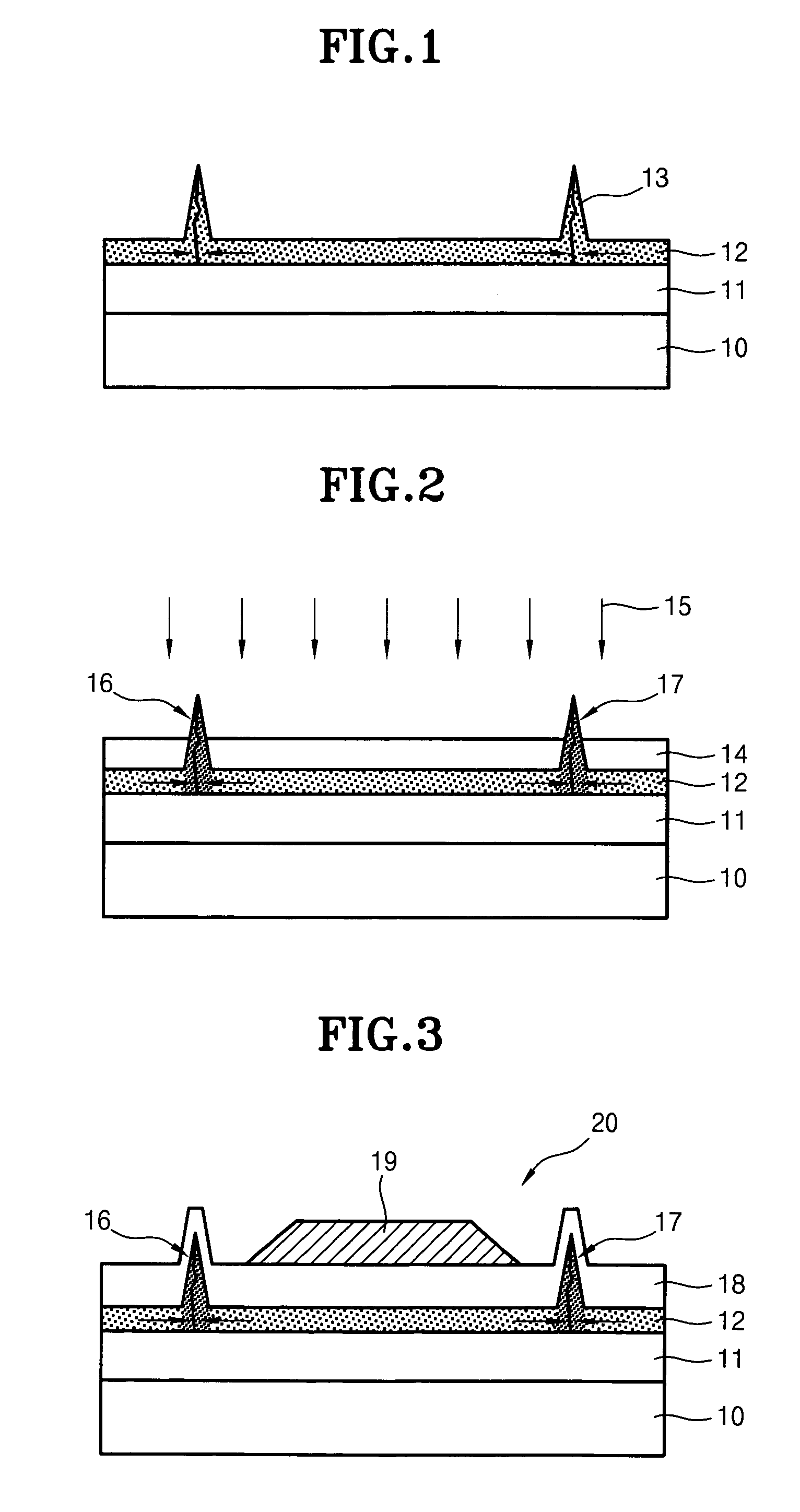
[0021]Hereinafter, a preferred embodiment of the present invention will be described with reference to the accompanying drawings.

[0022]First, according to the technical principle of the present invention, an a-Si layer is crystallized into a poly-Si layer by using the SLS method, and ions with a high concentration are then selectively implanted into a protrusion formed during crystallization into the poly-Si layer, so that the protrusion becomes a source / drain electrode and is excluded from a panel area which is a passage through which electrons and holes move.

[0023]As a result, the channel area of the TFT includes pure poly-Si without the protrusion, so that the mobility of the electrons and holes is not degraded when the TFT is operated. Therefore, the present invention can provide a poly-Si TFT having a superior characteristic.

[0024]FIGS. 1 through 3 are sectional views for describing steps of a method for forming a poly-Si TFT according to the present invention, which will be de...


PUM

PropertyMeasurementUnit
temperatureaaaaaaaaaa
areaaaaaaaaaaa
dielectricaaaaaaaaaa

Abstract

A method for forming a polycrystalline silicon thin film transistor. The method includes the steps of: forming a polycrystalline silicon layer including multiple protrusions by crystallizing the amorphous silicon layer according to a crystallization method in which the multiple protrusions are formed due to collision between crystal grains; patterning the polycrystalline silicon layer in an active pattern which includes only two protrusions of the multiple protrusions, which are apart from each other and located at both sides of a gate electrode-forming area; applying a barrier layer on the patterned polycrystalline silicon layer while partially covering the two protrusions; and forming a source electrode and a drain electrode at the protrusions of the polycrystalline silicon layer formed at both sides of the gate electrode-forming area by ion-implanting dopants into a resultant lamination.

Description

BACKGROUND OF THE INVENTION[0001]1. Field of the Invention[0002]The present invention relates to a method for manufacturing a thin film transistor liquid crystal display, and more particularly to a method for forming a polycrystalline silicon thin film transistor by using sequential lateral solidification.[0003]2. Description of the Prior Art[0004]As generally known in the art, a thin film transistor (hereinafter, referred to as “TFT”) used as a switching element in a liquid crystal display, an organic light emitting display, etc., is an element having the most important role in performance of such flat panel display devices. Here, the mobility or current leakage, which serves as a standard for determining the performance of the TFT, largely depends on the state or structure of the semiconductor active layer, which is a passage through which charge carriers move, or the state or structure of the silicon thin film which is material of the semiconductor active layer.[0005]Most TFTs of...

Claims


Application Information

Patent Timeline
Patent Type & Authority Patents(United States)
IPC IPC(8): H01L21/336
CPCH01L21/2022H01L27/1285H01L29/66757H01L29/04H01L27/1296H01L21/02422H01L21/02488H01L21/02678H01L21/02532H01L21/02587G02F1/136H01L21/02595H01L21/02667
Inventor SON, KYOUNG SEOKRYU, MYUNG KWANPARK, JAE CHULKIM, EOK SULEE, JUN HOKWON, SE YEOULIM, JANG SOON
Owner BOE HYDIS TECH CO LTD
Why Eureka
Try Eureka