
Silicon substrate as a light modulator sacrificial layer

Active Publication Date: 2006-04-11
SILICON LIGHT MACHINES CORP
View PDF881 Cites 83 Cited by
  • Summary
  • Abstract
  • Description
  • Claims
  • Application Information

AI Technical Summary

Benefits of technology

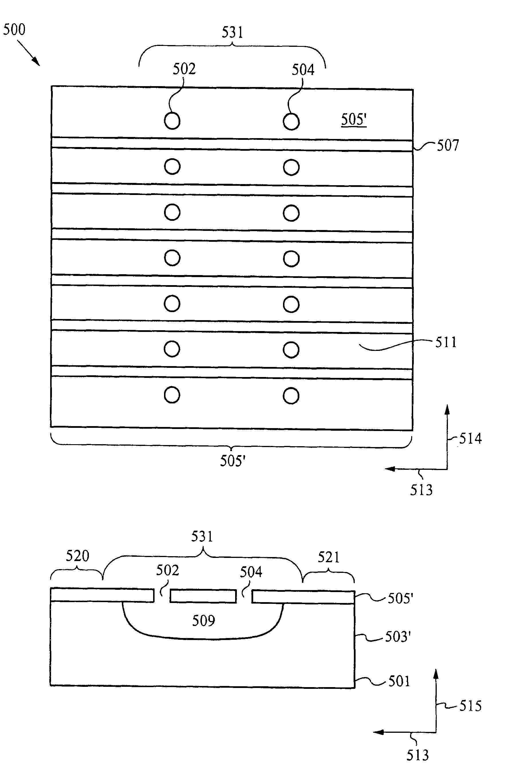
[0009]In still further embodiments of the invention, access holes and / or access trenches are formed through the ribbons prior to etching the cavity in the wafer substrate. The access holes and / or access trenches are formed in order to increase the local etching rate of the silicon wafer under the center portions, or active portions, of the ribbons.

Problems solved by technology

Firstly, fabrication can involve numerous time consuming steps, raising the cost of the devices.
Secondly, the dielectric materials typically used to fabricate these devices (silicon nitride and silicon oxide) result in devices which exhibit a propensity to charge.
Charging can perturb or shift the switching bias voltage required to operate the devices possibly leading to unreliable or irreproducible optical signals.
Thirdly, fabrication steps of these devices are often incompatible with materials and / or fabrication steps used to make integrated circuits.
Accordingly, optical MEM devices and integrated circuits generally need to be fabricated separately and then laboriously combined in subsequent steps.

Method used


Image

  • Silicon substrate as a light modulator sacrificial layer
  • Silicon substrate as a light modulator sacrificial layer
  • Silicon substrate as a light modulator sacrificial layer

Examples


Embodiment Construction

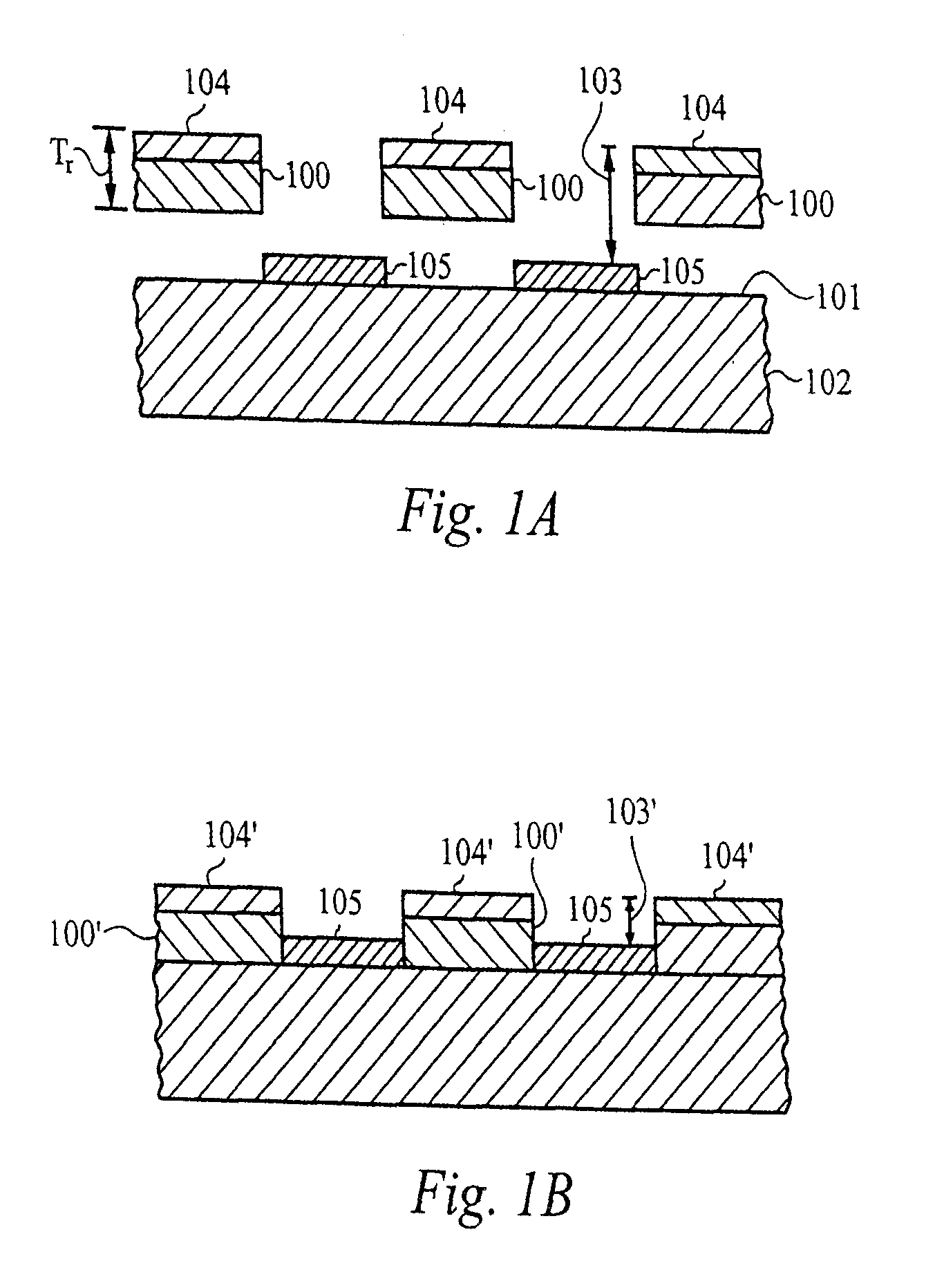
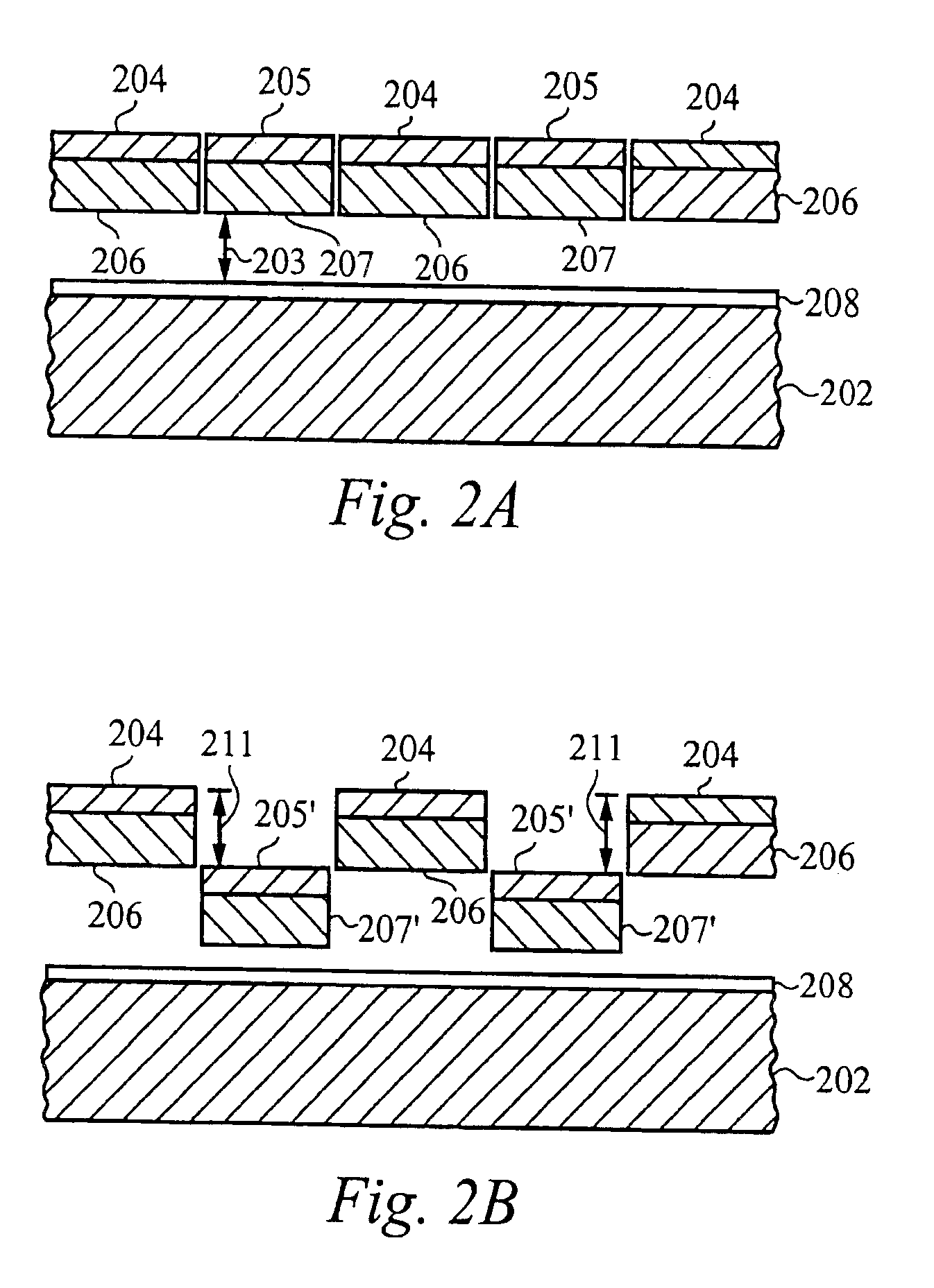
[0019]Referring to FIG. 1a, an optical MEM device can have a plurality of movable ribbons 100 with reflective surfaces 104 spatially arranged over a substrate 102 and a plurality of reflective surfaces 105 spatially arranged on the substrate 102 between movable ribbons 100, such that adjacent reflective surfaces 104 and 105 modulate light, as described below. The surfaces 104 and 105 are made to be reflective by depositing a thin film of reflective material, such as silver or aluminum, on the ribbons 100 and substrate 102, respectively. The ribbons 100 and the substrate 102 are preferably formed from silicon-based materials such as silicon nitride. A height difference 103 between the reflective surfaces 104 and 105 is preferably configured to be λ / 2 when the ribbons 100 are in an up position, as shown in FIG. 1a. When light having a wavelength λ impinges on the compliment of reflective surfaces 104 and 105, the light that is reflected from the surfaces 104 and 105 is in phase, there...


PUM


Abstract

An optical MEM device is fabricated with a patterned device layer formed on a silicon wafer. Preferably, the patterned device layer is patterned with plurality of ribbons and / or access trenches. The central portion of the ribbon is released from the silicon wafer using a selective etch process, wherein a cavity is formed under the central portion of the ribbon, while opposing ribbon ends remain attached to the wafer. The selective etching process preferably utilizes an enchant comprising xenon difluoride. In accordance with further embodiments, the silicon wafer is doped, patterned or otherwise modified to enhance the selectivity of the etching process.

Description

FIELD OF THE INVENTION[0001]The present invention relates to (micro-electro mechanical) MEM devices. More particularly, the present invention relates to controlled etch processes for fabricating optical MEM devices.BACKGROUND OF THE INVENTION[0002]Optical MEM devices are used to modulate one or more wavelengths of light. Optical MEM devices can have applications in display, print and electrical device technologies. Examples of optical MEM devices which utilize suspended micro-ribbon structures to modulate light are disclosed in the U.S. Pat. Nos. 5,311,360, 5,841,579 and 5,808,797, all issued to Bloom et al., the contents of which are hereby incorporated by reference.[0003]Briefly, an optical MEM device described in the above referenced patents has one or more sets of movable ribbons that comprise a support layer and a reflective top-layer. The support layer is preferably a silicon nitride layer and the reflective toplayer is preferably an aluminum layer. The ribbon structures are t...

Claims


Application Information

Patent Timeline
IPC IPC(8): G02B26/00G02B26/02G02B5/18
CPCG02B26/0808G02B5/1857
Inventor HUNTER, JAMESGUDEMAN, CHRISTOPHER S.
Owner SILICON LIGHT MACHINES CORP
Learn More