Microelectronic mechanical system structure forming method

A technology of microelectronic machinery and system structure, applied in microstructure technology, microstructure device, manufacturing microstructure device, etc., can solve the problems of reduced etching rate, difficult to control, fast etching rate, etc., to improve the removal rate, The effect of improving reliability

Inactive Publication Date: 2015-05-20
ACM RES SHANGHAI
View PDF8 Cites 2 Cited by
  • Summary
  • Abstract
  • Description
  • Claims
  • Application Information

AI Technical Summary

Problems solved by technology

However, since water is produced during the etching process, and water will accelerate the etching reaction, too much water residue will cause the etching rate to be too fast and difficult to control, increasing the unevenness of etching, so ethanol (water-absorbing agent) must be used ) takes water away, and the water is taken away, which will cause the etch rate to decrease, and the water produced may still make the movable structure in the MEMS device stick

Method used


Image

  • Microelectronic mechanical system structure forming method
  • Microelectronic mechanical system structure forming method
  • Microelectronic mechanical system structure forming method

Examples


Embodiment Construction

[0012] In order to describe the technical content, achieved goals and effects of the present invention in detail, the following will be described in detail in conjunction with the embodiments and accompanying drawings.

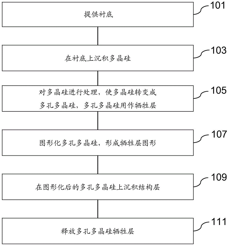
[0013] refer to figure 1 , discloses a flowchart of an embodiment of the MEMS structure forming method of the present invention. The method comprises the steps of:

[0014] Step S101, providing a substrate;

[0015] Step S103, depositing polysilicon on the substrate;

[0016] Step S105, processing the polysilicon to transform the polysilicon into porous polysilicon, and the porous polysilicon is used as a sacrificial layer;

[0017] Step S107, patterning the porous polysilicon to form a sacrificial layer pattern;

[0018] Step S109, depositing a structural layer on the patterned porous polysilicon;

[0019] Step S111 , releasing the porous polysilicon sacrificial layer.

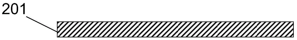
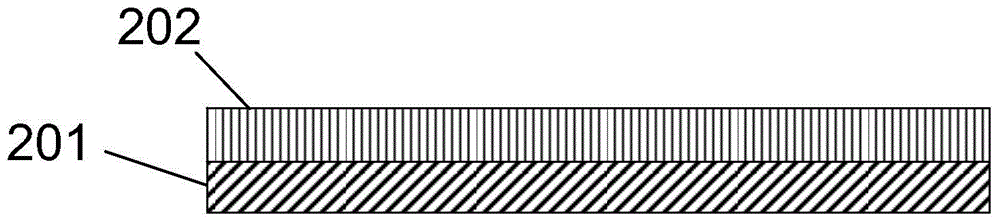
[0020] refer to Figure 2A-2I , reveals a schematic cross-sectional structure corr...


PUM


Abstract

The invention discloses a microelectronic mechanical system structure forming method, which comprises the following steps: providing a substrate; depositing polycrystalline silicon on the substrate; treating the polycrystalline silicon, so that the polycrystalline silicon is transformed into porous polycrystalline silicon, wherein the porous polycrystalline silicon is used as a sacrificial layer; imaging the porous polycrystalline silicon to form a sacrificial layer pattern; depositing a structure layer on the imaged porous polycrystalline silicon; and releasing the porous polycrystalline silicon sacrificial layer. The porous polycrystalline silicon is adopted as the sacrificial layer; and the sacrificial layer is in a pore form so that the removal rate of the sacrificial layer is improved. In addition, the porous polycrystalline silicon sacrificial layer can be released by adopting xenon difluoride; and a production product is in a gaseous state at room temperature and atmospheric pressure, so that the adhesion phenomenon is avoided; and the reliability of microelectronic mechanical system structure formation is improved.

Description

technical field [0001] The invention relates to the technical field of micro-electro-mechanical systems, in particular to a method for forming a micro-electro-mechanical system structure. Background technique [0002] With the rapid development of modern microelectronics technology, a new technology, Micro-Electro-Mechanical-System (MEMS, Micro-Electro-Mechanical-System) is emerging. MEMS technology integrates microelectronics technology and precision machining technology to realize the integration of microelectronics and machinery. MEMS technology has the advantages of miniaturization, stable performance, integration, and low power consumption, so it has begun to be widely used in many fields. MEMS structures, such as suspension bridge structures, cavity structures, etc., are widely used structures in the MEMS field, which are formed using a sacrificial layer release process. The process includes depositing a sacrificial oxide layer over the substrate, patterning the sacr...

Claims


Application Information

Patent Timeline
Patent Type & Authority Applications(China)
IPC IPC(8): B81C1/00
Inventor 肖东风贾照伟王坚王晖
Owner ACM RES SHANGHAI
Why Eureka
Try Eureka