Structured screens for controlled spreading of light

a structured screen and light technology, applied in the field of optical devices, can solve the problems of limited shaping over the resulting scattering, inability to achieve such accuracy, and inability to control the spreading pattern only to a limited degree, so as to achieve the effect of increasing numerical aperture and increasing peak intensity

Inactive Publication Date: 2006-04-25
CORNING INC
View PDF76 Cites 64 Cited by
  • Summary
  • Abstract
  • Description
  • Claims
  • Application Information

AI Technical Summary

Benefits of technology

[0026]In view of the foregoing, it is an object of the present invention to provide a structured screen surface that addresses the drawbacks mentioned above by allowing control of the elementary structures (microstructures) that define the surface as well as their relative distribution across the surface of the device. The control of surface shape and relative spatial arrangement is completely deterministic, in contrast with the prior art which relies on statistical control and placement of microstructures. With the approach of the invention it is possible to modify the quality of the light spreading process so as to make it appropriate and useful in a wide range of applications.
[0036]In accordance with another of its aspects, the invention provides apparatus for controlled spreading of light comprising a plurality of microstructures, each microstructure being located with better than 10·λn accuracy at a predetermined location with respect to all other microstructures and each microstructure having a configuration that corresponds, with better than 10·λn accuracy, to a predetermined mathematical relation, where λn is the nominal operating wavelength of the apparatus and said predetermined locations and predetermined mathematical relations allow an a priori calculation of the spreading of incident light by the apparatus.
[0065](b) a plurality of microstructures distributed over at least some of said plurality of surfaces, said plurality of microstructures serving to control the spread of light incident on the structured screen.

Problems solved by technology

Methods based on statistical processes are unable to attain such accuracy and, for that reason, can control the spreading pattern only to a limited degree.
If only limited control is possible over the screen structure, only limited shaping is possible over the resulting scattering.

Method used


Image

  • Structured screens for controlled spreading of light
  • Structured screens for controlled spreading of light
  • Structured screens for controlled spreading of light

Examples


example 1

Effect of Microstructure Shape

[0177]This example illustrates the importance of the shape of each microstructure in tailoring the light spreading pattern.

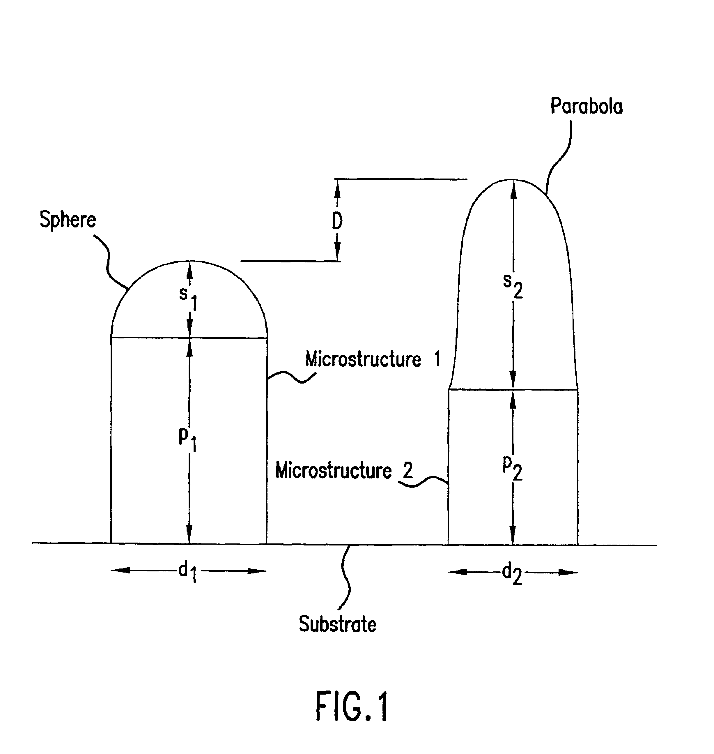
[0178]Initially we consider a regular array of identical microstructures with a shape that can be expressed as function of one or more parameters, some of which are random variables. For instance, a microstructure of spherical shape has a sag function that is given by R−(R2−r2)½, where R denotes the radius of curvature and r denotes the radial position from the origin. According to this definition, the array consists of spherical microlenses with possibly variable radii of curvature. The size of each microstructure is identical throughout the screen surface, so that the presence of randomness is confined to a particular parameter, namely, the radii of curvature of the spherical microlenses.

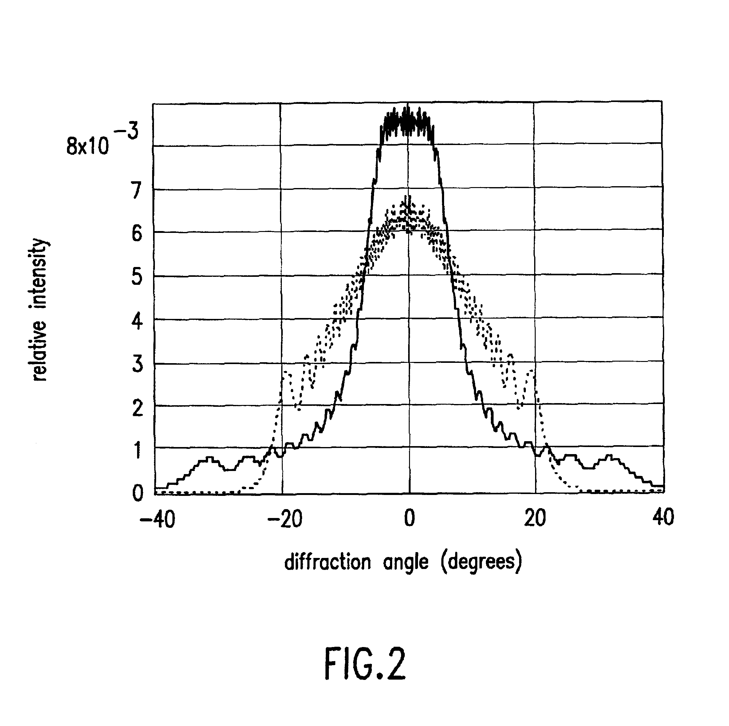
[0179]Consider initially a screen made of silicon to operate in the infrared in a wavelength range from 2 to 4 microns. FIG. 26 shows the far-fie...

example 2

Effect of Vertical Offset

[0187]As illustrated in Example 1, the microstructure profile basically determines the shape and the divergence span of the scattering pattern. Randomizing the profile helps reduce the high-frequency oscillations and attain a smoother pattern. Depending on the spectral band of operation, hot spots may occur that are detrimental to the performance of the screen (see, for example, FIG. 26).

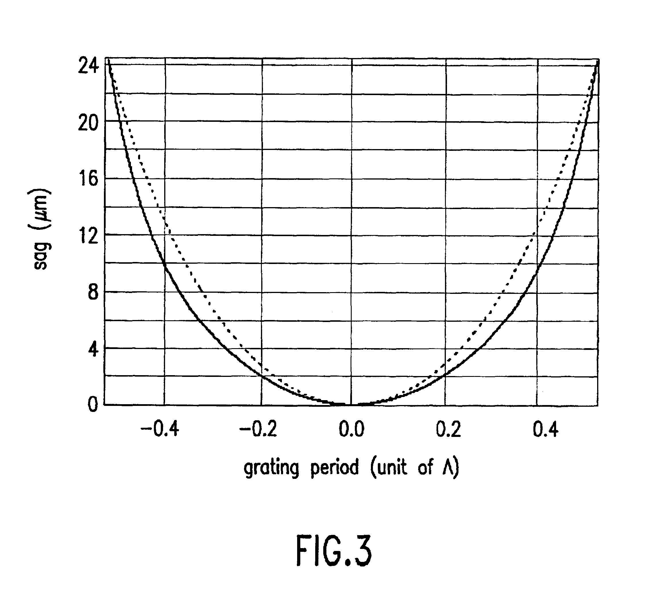
[0188]An important element useful in homogenizing the scattering pattern and providing a further parameter to help decrease the influence of hot spots is the vertical offset or piston of the microlens. Its effect is basically to displace a microlens along its axis of symmetry by a definite quantity. The net result is that the relative position of the vertex or origin of a microstructure varies as a function of its position on the screen.

[0189]To illustrate the effect, we again consider the array used to generate FIG. 26, that is, spherical microlenses of diameter 100 microns...

example 3

Spatial Arrangement of Microstructures

[0192]A defining global parameter of great relevance to the scattering pattern is the spatial arrangement of the microstructures on the screen. The main influence of the spatial arrangement is reflected in the overall symmetry of the scattering pattern.

[0193]For instance, the regular square array of FIG. 36 generates a three-dimensional pattern that resembles a rectangle, depending on the divergence angles introduced by the local configuration of the microlenses. The hexagonal array of FIG. 37, on the other hand, generates a scattering pattern in the form of a hexagon which can be stretched along one direction more than another depending on the divergence angles introduced by the configuration of the microlenses.

[0194]Apart from geometrical considerations, the overall symmetry is important in many aspects, but mainly because it affects how energy is concentrated in the observation plane. For instance, for a pattern of similar spatial extension, ...


PUM

PropertyMeasurementUnit
depthaaaaaaaaaa
diameteraaaaaaaaaa
diameteraaaaaaaaaa

Abstract

Structured screens for the controlled spreading, diffusion, or scattering of an incident beam are provided. The screens are composed of microstructures (1,2) whose configurations and distribution on the surfaces of the screen are precisely determined. In certain embodiments, the configurations and / or their distribution is randomized. The structured screens can be used as diffusing screens or display screens.

Description

CROSS REFERENCE TO RELATED PROVISIONAL APPLICATION[0001]This application claims the benefit under 35 USC §119(e) of U.S. Provisional Application No. 60 / 222,033 filed Jul. 31, 2000, the content of which in its entirety is hereby incorporated by reference.I. FIELD OF THE INVENTION[0002]The present invention discloses an optical device composed of a substrate whose surface or surfaces, which may be flat or curved, contain a distribution of microstructures capable of spreading (also referred to herein as “diffusing” or “scattering”) an incident beam over a controlled range of angles and with controllable intensity variation across the useful field. The said device is referred to herein as a “structured screen” or simply a “screen.”[0003]The structured screens of the invention have a plurality of applications which generally fall into two major categories, namely, diffusive screens and display screens. More particularly, applications of the structured screens include, but are not limited...

Claims


Application Information

Patent Timeline
Patent Type & Authority Patents(United States)
IPC IPC(8): G02B5/02G02B3/00G03B21/62G02B3/08G02B5/18G02F1/1335
CPCG02B3/0043G02B3/0056G02B3/0068G02B3/04G02B3/08G02B5/0221G02B5/0252G02B5/0268G02B5/0278G02B5/1871G02B5/0215Y10S430/146G02B5/02
Inventor MORRIS, G. MICHAELSALES, TASSO R. M.
Owner CORNING INC
Why Eureka
Try Eureka