Gap filling with a composite layer

a composite layer and gap filling technology, applied in the direction of basic electric elements, semiconductor/solid-state device manufacturing, electric apparatus, etc., can solve the problems of affecting device operation and requiring semiconductor manufacturers to fill completely

Inactive Publication Date: 2006-04-25
APPLIED MATERIALS INC
View PDF11 Cites 45 Cited by
  • Summary
  • Abstract
  • Description
  • Claims
  • Application Information

AI Technical Summary

Problems solved by technology

Gaps having a combination of high aspect ratio and a small width present a particular challenge for semiconductor manufacturers to fill completely.
In short, the challenge usually is to prevent the deposited film from growing in a manner that closes off the gap before it is filled.
Failure to fill the gap completely results in the formation of voids in the deposited layer, which may adversely affect device operation such as by trapping undesirable impurities.

Method used


Image

  • Gap filling with a composite layer
  • Gap filling with a composite layer
  • Gap filling with a composite layer

Examples


Embodiment Construction

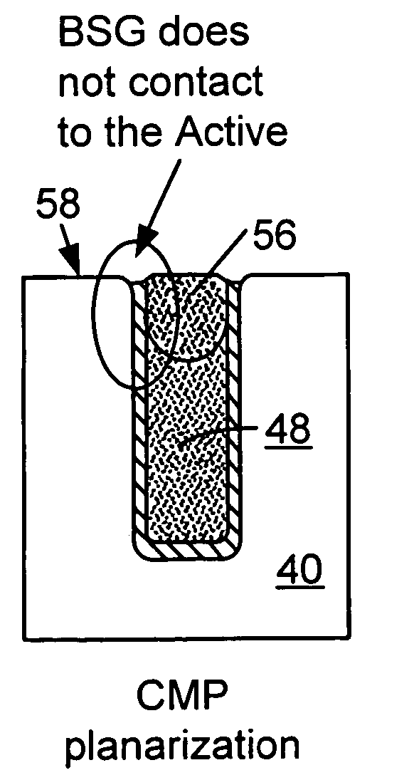
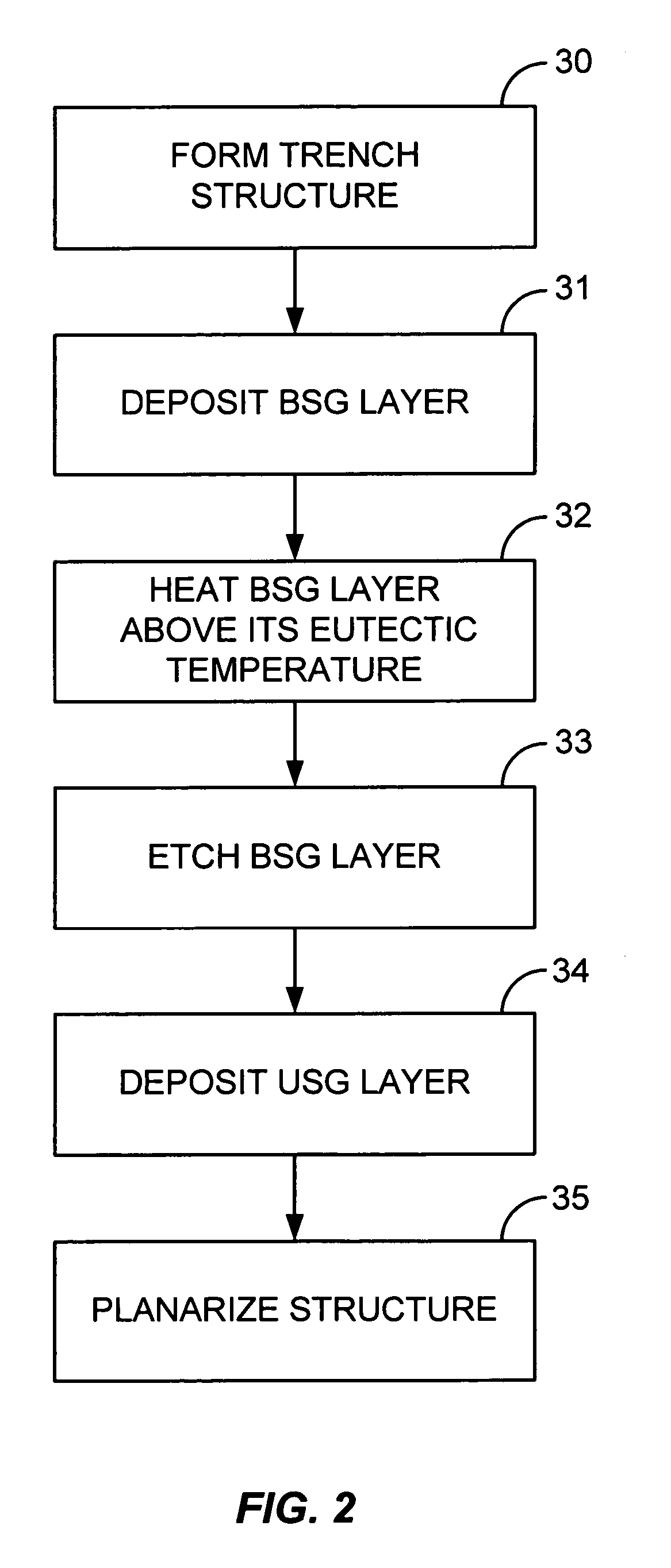
[0019]Embodiments of the invention fill trenches and / or gaps between adjacent raised features of integrated circuits by depositing a composite insulating material, such as silicon oxide material, into the trenches and / or gaps. The inventors have developed a method of depositing the composite material using a multistep process. In one embodiment the multistep process includes a depositing a first boron-doped silicon oxide layer (also referred to as borosilcate glass or BSG layer) using a thermal CVD technique, heating the deposited BSG layer above its Eutectic temperature and then depositing a second undoped silicon oxide layer (or USG layer) over the BSG layer using a plasma CVD technique. The multistep process can be used to fill the STI trenches in a manner that is superior to using a single layer alone. Embodiments of the invention permit the dielectric material to be deposited with substantially 100% gapfill for integrated circuits having minimum feature sizes of 0.10 μm or less...


PUM

PropertyMeasurementUnit
temperatureaaaaaaaaaa
pressureaaaaaaaaaa
pressureaaaaaaaaaa

Abstract

A method of filling a gap formed between adjacent raised surfaces on a substrate. In one embodiment the method comprises depositing a boron-doped silica glass (BSG) layer over the substrate to partially fill the gap using a thermal CVD process; exposing the BSG layer to a steam ambient at a temperature above the BSG layer's Eutectic temperature; removing an upper portion of the BSG layer by exposing the layer to a fluorine-containing etchant; and depositing an undoped silica glass (USG) layer over the BSG layer to fill the remainder of the gap.

Description

BACKGROUND OF THE INVENTION[0001]One of the primary steps in the fabrication of modern semiconductor devices is the formation of a thin film on a semiconductor substrate by chemical reaction of gases. Such a deposition process is referred to generally as chemical vapor deposition (“CVD”). Conventional thermal CVD processes supply reactive gases to the substrate surface, where heat-induced chemical reactions take place to produce a desired film. Plasma-enhanced CVD (“PECVD”) techniques, on the other hand, promote excitation and / or dissociation of the reactant gases by the application of radio-frequency (“RF”) energy to a reaction zone near the substrate surface, thereby creating a plasma.[0002]Any of these CVD techniques may be used to deposit conductive or insulative films during the fabrication of integrated circuits. For applications such as the deposition of insulating films as premetal or intermetal dielectric layers in an integrated circuit or for shallow trench isolation, one ...

Claims


Application Information

Patent Timeline
Patent Type & Authority Patents(United States)
IPC IPC(8): H01L21/311H01L21/76H01L21/762
CPCH01L21/76224
Inventor BYUN, JEONG SOOYUAN, ZHENGVENKATARAMAN, SHANKARKARIM, M. ZIAULPHAM, THANH N.YIEH, ELLIE Y.
Owner APPLIED MATERIALS INC
Why Eureka
Try Eureka