Thin-film transistor, method of manufacturing the same, and display device

a technology of thin film transistors and transistors, which is applied in the direction of transistors, semiconductor devices, electrical devices, etc., can solve the problems of more chance of short-circuit between wirings, increased risk of short-circuit, and fluctuation of voltage, so as to improve the quality of display, stabilize the characteristic, and reduce the parasitic capacitance

Active Publication Date: 2011-10-06
JOLED INC
View PDF11 Cites 186 Cited by
  • Summary
  • Abstract
  • Description
  • Claims
  • Application Information

AI Technical Summary

Benefits of technology

[0052]According to each of the thin-film transistors of the embodiments, the low-resistance region, which includes one or more elements selected from the group consisting of aluminum, boron, gallium, indium, titanium, silicon, germanium, tin, and lead as a dopant, or includes the oxygen concentration which is lower than the oxygen concentration of the channel region, is provided in at least a part of each of the source region and the drain region extending in the depth di

Problems solved by technology

However, when a parasitic capacitance generated in a cross region of a gate electrode and a source electrode, or of the gate electrode and a drain electrode of the thin-film transistor is large, the signal voltage may fluctuate, leading to an occurrence of image degradation.
As a result, there is more chance of short-circuit between the wirings etc., and ther

Method used


Image

  • Thin-film transistor, method of manufacturing the same, and display device
  • Thin-film transistor, method of manufacturing the same, and display device
  • Thin-film transistor, method of manufacturing the same, and display device

Examples


first embodiment

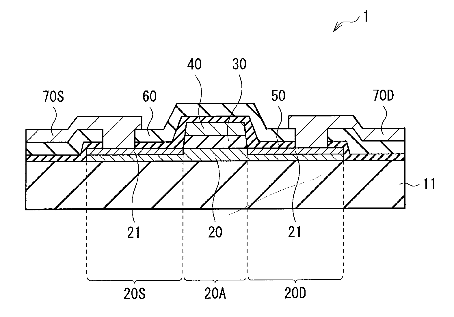
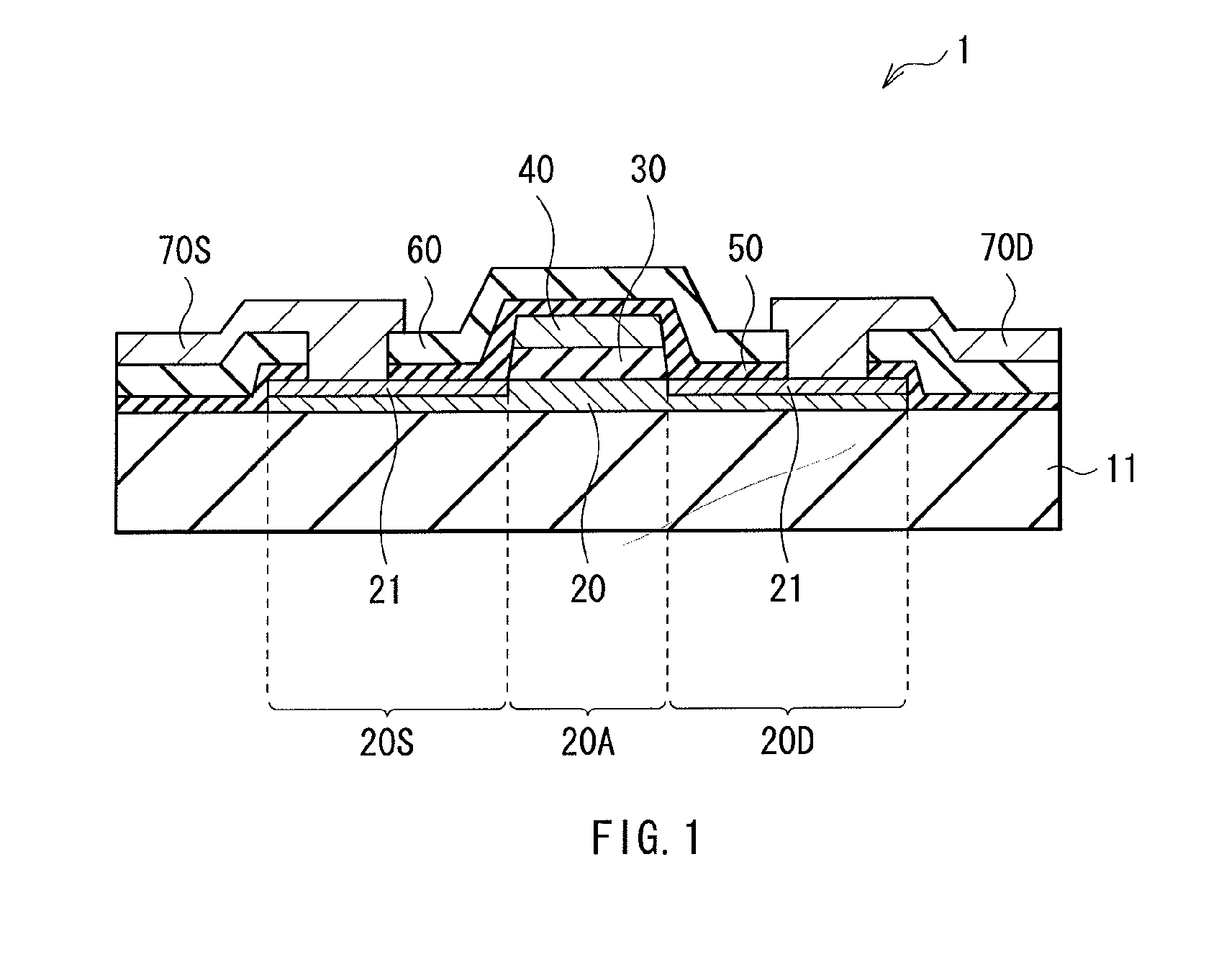
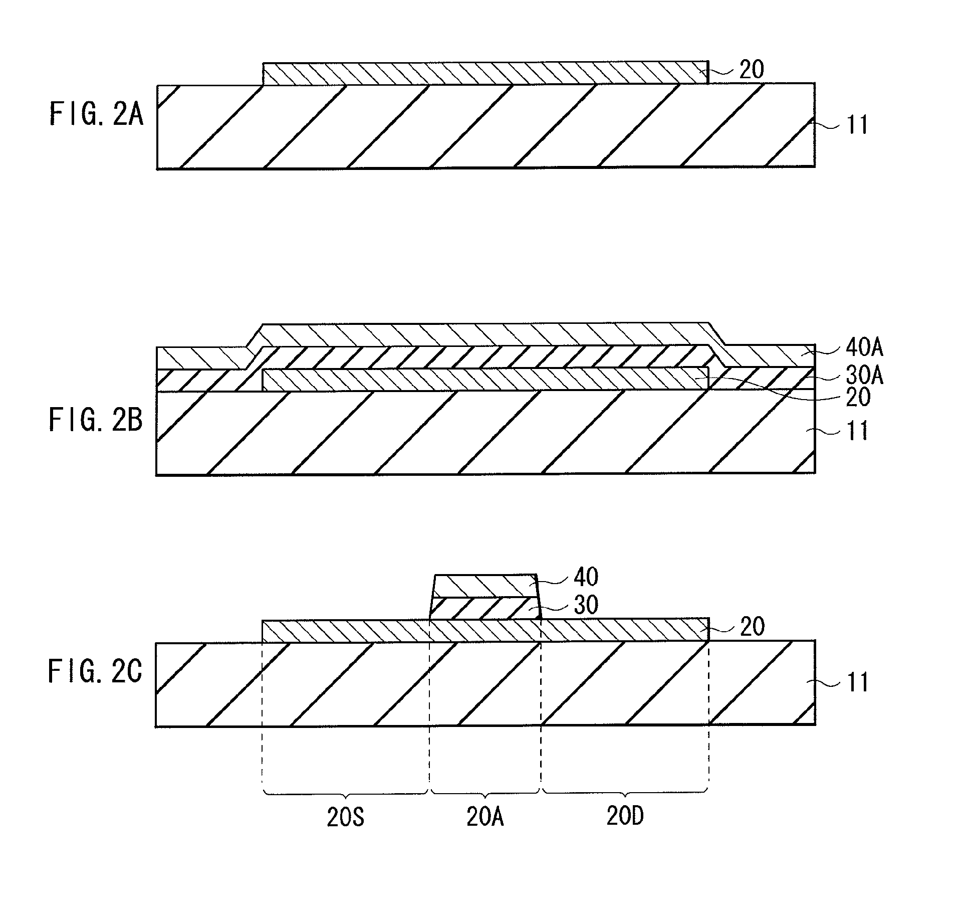
[0104]FIG. 1 illustrates a cross-sectional configuration of a thin-film transistor 1 according to a first embodiment. The thin-film transistor 1 may be used as a drive element in a device such as a liquid crystal display and an organic EL display. The thin-film transistor 1 may have a top-gate structure (or a staggered structure), in which an oxide semiconductor film 20, a gate insulating film 30, a gate electrode 40, a high-resistance film 50, an interlayer insulating film 60, a source electrode 70S, and a drain electrode 70D are stacked in this order on a substrate 11, for example.

[0105]The substrate 11 may be configured by a glass substrate, a plastic film, or other suitable member, for example. A material of a plastic can be polyethylene terephthalate (PET), polyethylene naphthalate (PEN), or other suitable material. The plastic film, which is inexpensive, may be used in order to deposit the oxide semiconductor film 20 without heating the substrate 11 in a later-described sputte...

second embodiment

[0141]A thin-film transistor according to a second embodiment has a similar configuration as that of the thin-film transistor 1 according to the first embodiment illustrated in FIG. 1, except that a configuration and a manufacturing method of the low-resistance region 21 are different from those in the first embodiment described above. Note that the same or equivalent elements as those according to the first embodiment are denoted with the same reference numerals, and will not be described in detail. Also, process steps corresponding to those in the first embodiment will be described with reference to FIGS. 1 to 3C.

[0142]In the thin-film transistor according to this embodiment, the low-resistance region 21 is made low in resistance by containing one or more elements selected from a group including aluminum (Al), boron (B), gallium (Ga), indium (In), titanium (Ti), silicon (Si), germanium (Ge), tin (Sn), and lead (Pb) as a dopant. Thin-film transistor 1 is thereby able to have the se...

third embodiment

[0159]FIG. 9 illustrates a cross-sectional configuration of a thin-film transistor 1B according to a third embodiment. The thin-film transistor 1B has a similar configuration as that of the thin-film transistor 1 according to the first embodiment described above, except that the thin-film transistor 1B is a bottom-gate thin-film transistor in which the gate electrode 40, the gate insulating film 30, the oxide semiconductor film 20, a channel protecting film 80, the interlayer insulating film 60, the source electrode 70S, and the drain electrode 70D are stacked in this order on the substrate 11. Note that the same or equivalent elements as those according to the first embodiment are denoted with the same reference numerals, and will not be described in detail.

[0160]The channel protecting film 80 is provided on the channel region 20A of the oxide semiconductor film 20. The channel protecting film 80 may have a thickness of about 200 nm, and may be configured of a monolayer film, which...


PUM


Abstract

A thin film transistor is provided. The thin film transistor includes an oxide semiconductor layer including a source region, a drain region, and a channel region wherein a portion of the source and drain regions has an oxygen concentration less than the channel region. Further provided is a thin film transistor that includes an oxide semiconductor layer including a source region, a drain region, and a channel region, wherein a portion of the source and drain regions includes a dopant selected from the group consisting of aluminum, boron, gallium, indium, titanium, silicon, germanium, tin, lead, and combinations thereof.

Description

CROSS REFERENCES TO RELATED APPLICATIONS[0001]The present application claims priority to Japanese Priority Patent Application Nos. JP 2010-079293 and JP 2010-245035 filed in the Japan Patent Office on Mar. 30, 2010 and Nov. 1, 2010, respectively, the entire contents of which are hereby incorporated by reference.BACKGROUND[0002]The present application relates to a thin-film transistor using an oxide semiconductor, to a method of manufacturing the same, and to a display device provided with the thin-film transistor.[0003]An active-driving-type liquid crystal display device and an active-driving-type organic electroluminescence (hereinafter simply referred to as “EL”) display device each use a thin-film transistor (TFT) as a drive element, and each cause an electric charge, which corresponds to a signal voltage for writing an image, to be held in a hold capacitor. However, when a parasitic capacitance generated in a cross region of a gate electrode and a source electrode, or of the gat...

Claims


Application Information

Patent Timeline
IPC IPC(8): H01L29/786
CPCH01L29/41733H01L29/66969H01L29/7869H01L29/78618H01L29/45H01L29/66742H01L29/78696
Inventor MOROSAWA, NARIHIROOSHIMA, YOSHIHIRO
Owner JOLED INC
Why Eureka
Try Eureka