Semiconductor sensor, comprising a pixel structure and the use of said sensor in a vacuum system

a semiconductor sensor and vacuum system technology, applied in the field of semiconductor sensor with pixel structure, can solve the problems of sensor surface, system forced open, known image converters react sensiblely to electrons, etc., and achieve the effects of avoiding undesirable signals, good conductivity and light-imperviousness, and easy application

Inactive Publication Date: 2006-04-25
RHEINMETALL DEFENCE ELECTRONICS
View PDF19 Cites 14 Cited by
  • Summary
  • Abstract
  • Description
  • Claims
  • Application Information

AI Technical Summary

Benefits of technology

[0016]The layers preferentially consist of a conductive, light-impervious material, for example metal. Incident electrons are absorbed by the conductive material and led to the semiconductor structure. The light-impervious material prevents hazardous photons from penetrating the sensor surface, and undesirable signals are thus avoided. The layers preferentially

Problems solved by technology

A disadvantage, however, is that the known image converters react sensible against electrons that striking the sensor surface.
The kinetic energy of the electrons influences the crystalline semiconductor structure, so that the system is forced open under operation with the result of pixel defects, which show

Method used


Image

  • Semiconductor sensor, comprising a pixel structure and the use of said sensor in a vacuum system
  • Semiconductor sensor, comprising a pixel structure and the use of said sensor in a vacuum system
  • Semiconductor sensor, comprising a pixel structure and the use of said sensor in a vacuum system

Examples


Embodiment Construction

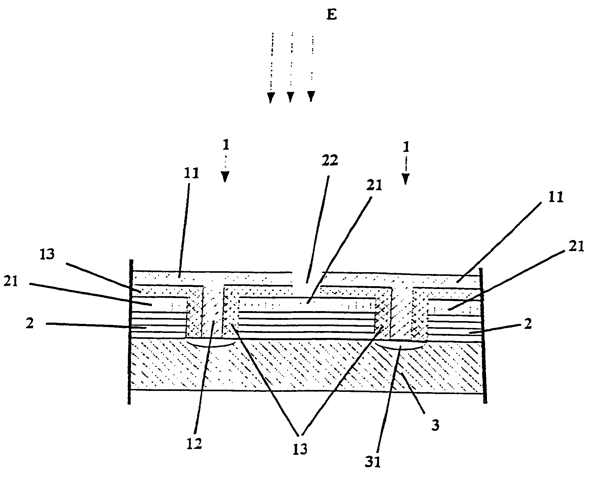
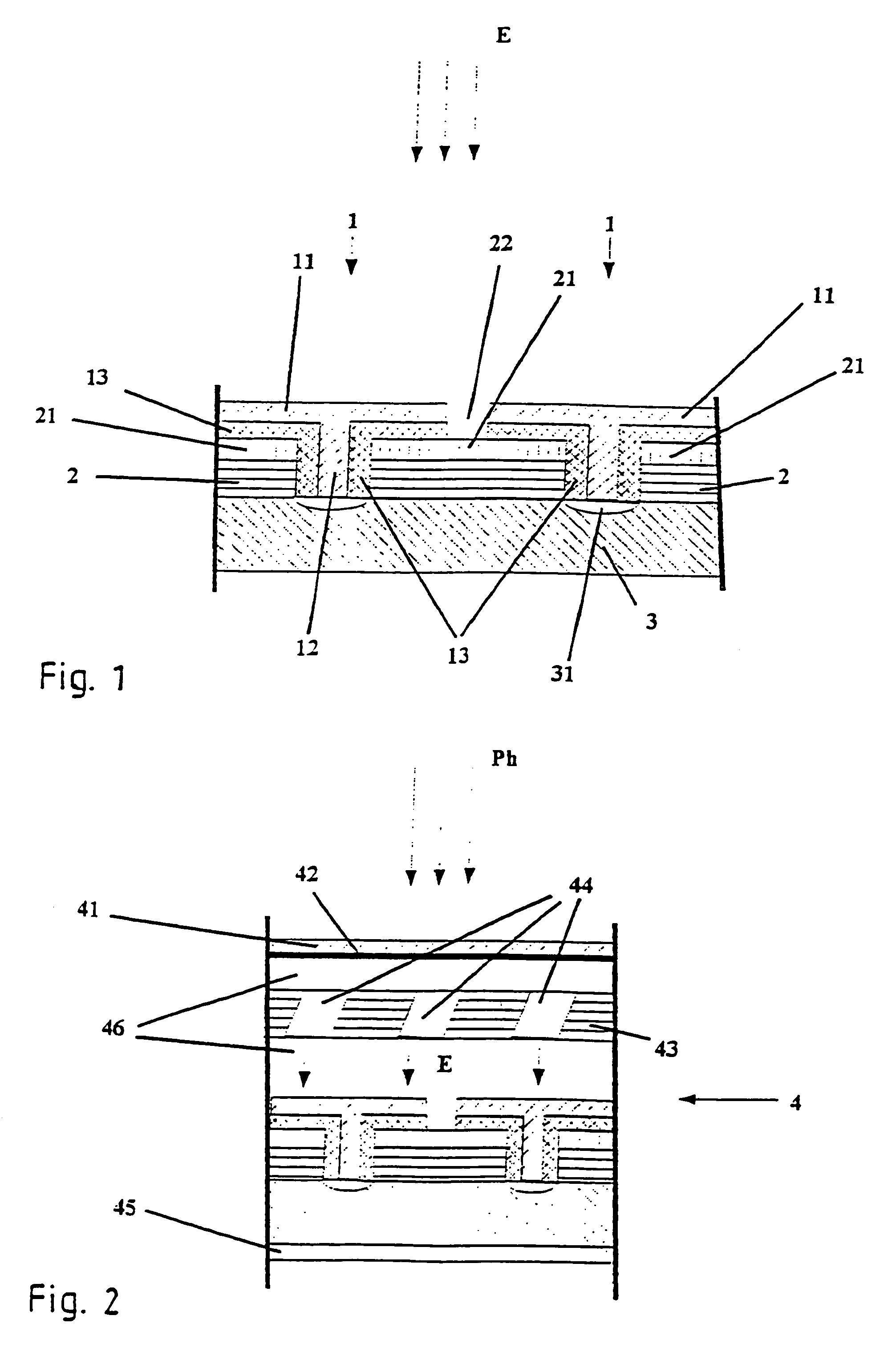
[0027]In FIG. 1 a part of a semiconductor sensor with two pixels is shown. On the sensor's surface that shows into the direction of the electron flow which is to be detected, in FIG. 1 above, conductive layers, which are assigned to the pixel structure 1, are assembled as active pixel surfaces 11, that preferably consist of aluminum. This conductive layer 11 is through-connected to a semiconductor element 3.

[0028]The semiconductor element 3 also has a pixel structure 1, which reproduces an assigned circuit for each pixel surface 11 that consists of conductive material. Besides the not shown semiconductor element 3 can be designed as active-pixel-structure. Between the conductive layer 11 of each pixel and the semiconductor element 3 an insulation 13 is planned with the exception of contact 12.

[0029]The insulation 13 separates the sensor surface 11 which is contacted 12 to the semiconductor element 1 from a second conductive layer 21 which screens the gaps between the pixel surfaces ...


PUM


Abstract

A semiconductor sensor for direct detection of electrons has a pixel structure in which a capacitance is designed to each pixel that stores a charge and converts the charge into a readable voltage. A conductive layer substantially covers the pixel structure. The conductive layer includes pixel surface coatings, each of which cover an individual pixel. Each pixel surface coating is separated from each adjoining pixel surface coating by a gap. A second conductive layer covers a surface of the gap. An insulation insulates the pixel surface coating from the second conductive layer. The conductive layers may be metal or other conductive, light impervious materials. The second conductive layer may include a capacitor electrode.

Description

CROSS REFERENCE TO RELATED APPLICATIONS[0001]Applicant claims priority under 35 U.S.C. §119 of German Application No. 199 27 694.3 filed Jun. 17, 1999. Applicant also claims priority under 35 U.S.C. §365 of PCT / DE00 / 01934 filed Jun. 13, 2000. The international application under PCT article 21(2) was not published in English.BACKGROUND OF THE INVENTION[0002]1. Field of the Invention[0003]The invention is a semiconductor sensor with pixel structure, containing a capacity for each pixel which stores charge and converts it into voltage that can be read out. The pixel structure is in the main completely covered with a conductive layer. Furthermore the invention is about the sensor's use integrated in a vacuum system (IC) with photo cathode. The semiconductor is ideal for image processing in opto-electronic applications.[0004]2. Prior Art[0005]Opto-electronic image converters are known in semiconductor technology. With the so-called CCD-device electrons are removed from the lattice struct...

Claims


Application Information

Patent Timeline
IPC IPC(8): H01L23/58G21K4/00H01L31/00H01J31/48H01J31/49H01L27/146
CPCH01J31/48H01L27/14665H01J31/49H01J2231/50068
Inventor FINK, LUTZ
Owner RHEINMETALL DEFENCE ELECTRONICS
Why Eureka
Try Eureka