Advanced wafer planarizing

a technology of advanced wafers and wafers, applied in the direction of total factory control, programme control, lapping machines, etc., can solve the problems of increasing the cost of manufacture, the control of the finishing and/or planarizing step is very complex, and the manufacturing cost of the planarizing and/or finishing step is also complex, so as to reduce the cost of manufacture, the control of the finishing and/or planarizing step is very complex, and the cost of manufacturing is increased.

Inactive Publication Date: 2006-05-02
SEMCON TECH
View PDF32 Cites 29 Cited by
  • Summary
  • Abstract
  • Description
  • Claims
  • Application Information

AI Technical Summary

Benefits of technology

[0006]There is a need to develop a control subsystem, more preferably an in situ control subsystem, which changes the cost of manufacture for a planarizing step. As discussed above, there is a need for an real time control for planarizing and / or polishing methods which change, more preferably improve, the cost of manufacture for a planarizing and / or a polishing step. There is a need for planarizing method which controls the planarizing using a cost of manufacture model. There is a need for planarizing method which controls the planarizing using a business model. There is a need for a cost of manufacture model which tracks the semiconductor wafer during its various planarizing steps and uses a cost of manufacture model appropriate to that individual planarizing step. There is a need for operative sensors which monitor the planarizing in a manner that improves the ability to control and improve the cost of manufacture for a particular finishing step.
[0007]It is an advantage of this invention to develop a control subsystem, more preferably an in situ control subsystem, which changes the cost of manufacture for a planarizing step. It is an advantage of this invention to develop a control subsystem, more preferably an in situ control subsystem, which improves the cost of manufacture for a planarizing step. It is an advantage of this invention to develop in some preferred embodiments an in situ control subsystem which can change the cost of manufacture for a planarizing step. It is an advantage of this invention to develop a planarizing method which improves control of planarizing and / or finishing during refining using a cost of manufacture parameters. It is an advantage of this invention to develop a method to use metrics related to cost of manufacture to improve control of the semiconductor wafer cost during its various planarizing steps and to use this control to change, more preferably improve, the manufacturing cost in situ at one or more individual planarizing steps. It is an advantage of this invention to develop a preferred method which uses preferred operative sensors which monitor the planarizing in a manner that improves the ability to control and improve the cost of manufacture for multiple planarizing steps and / or particular planarizing steps. Further, merely controlling planarizing in a manner that stops planarizing and / or polishing at the endpoint, misses a particularly preferred aspect of controlling the polishing process itself during a time period where defects such as microscratches, other unwanted surface defects, and unwanted costs can occur. It is generally an advantage of the improved control herein to improve the planarizing and planarizing control while also changing, more preferably reducing, the cost of manufacture of the workpiece. Improved real time control is particularly preferred.

Problems solved by technology

Current applicant evaluations show that the control of the finishing and / or planarizing step is very complex.
The optimizing of one control parameter to improve the control parameter's direct effect on cost of manufacture can have other generally unintended results which increase the cost of manufacture rather than the generally intended effect of decreasing the cost of manufacture.
The manufacturing cost for the planarizing and / or finishing step is also complex.
Cost of manufacture parameters can have different response surfaces to changes in control parameters thus making easy predictions on the overall cost effect generally very difficult.
Still further some parameters can be changed which improve yields but reduce the semiconductor wafer throughput enough to raise the cost of manufacture for each semiconductor wafer.
Still further, some costs can vary by customer or even by customer order (such as setup costs, overtime, shipping, packaging, etc.).
Further, merely controlling planarizing in a manner that stops planarizing and / or polishing at the endpoint, misses a particularly preferred aspect of controlling the polishing process itself during a time period where defects such as microscratches, other unwanted surface defects, and unwanted costs can occur.

Method used


Image

  • Advanced wafer planarizing
  • Advanced wafer planarizing
  • Advanced wafer planarizing

Examples


Embodiment Construction

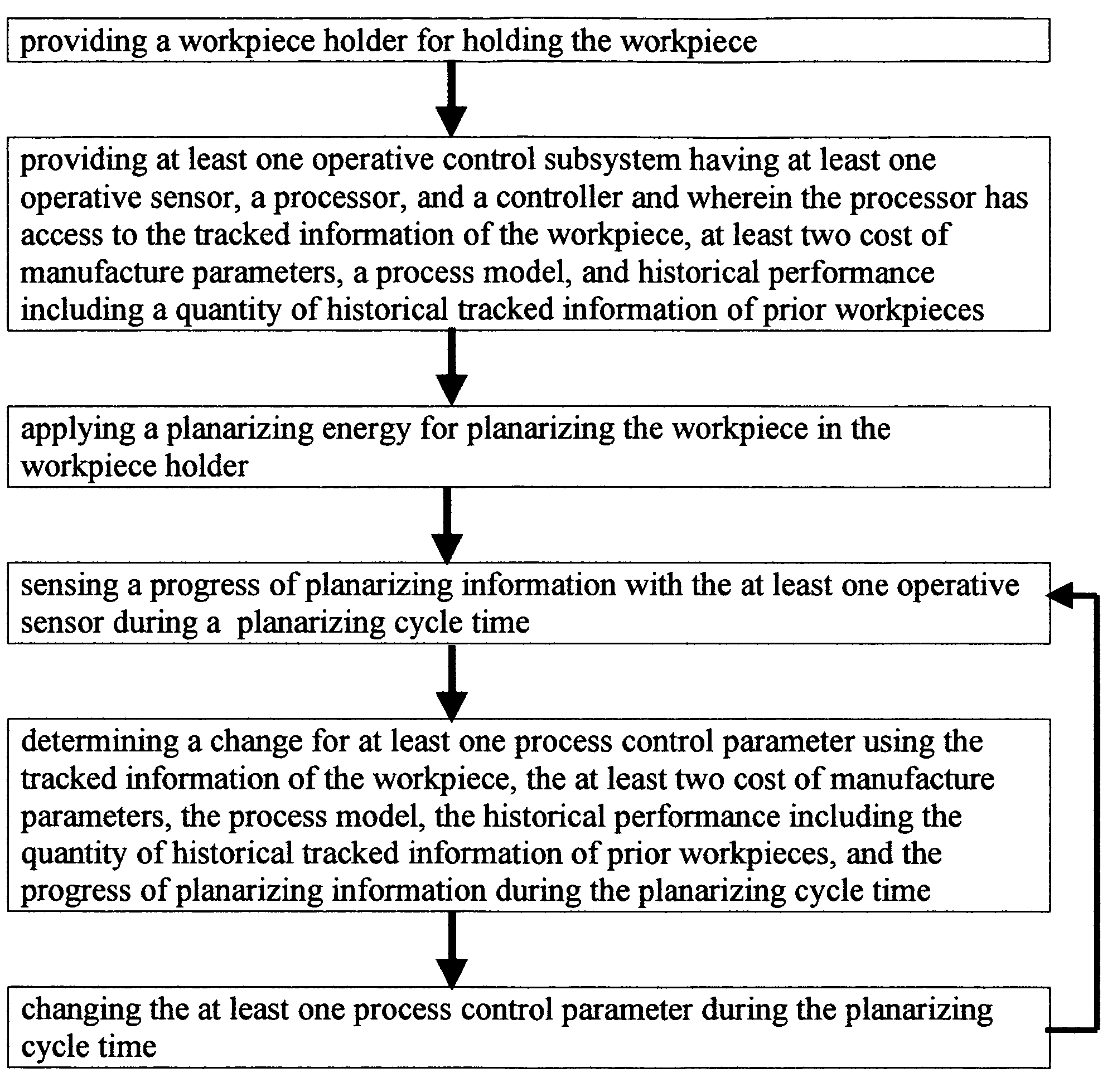
[0099]The semiconductor industry is in a relentless journey to increase computing power and decrease costs. Planarizing of a semiconductor wafer using in situ calculations of cost of manufacture parameters to improve control of finishing parameters can help simultaneously to decrease cost and reduce unwanted defects. Real time control of the planarizing energy on the semiconductor wafer surface using cost of manufacture parameters for real time optimization is particularly useful and preferred to help to change and / or reduce cost of manufacture.

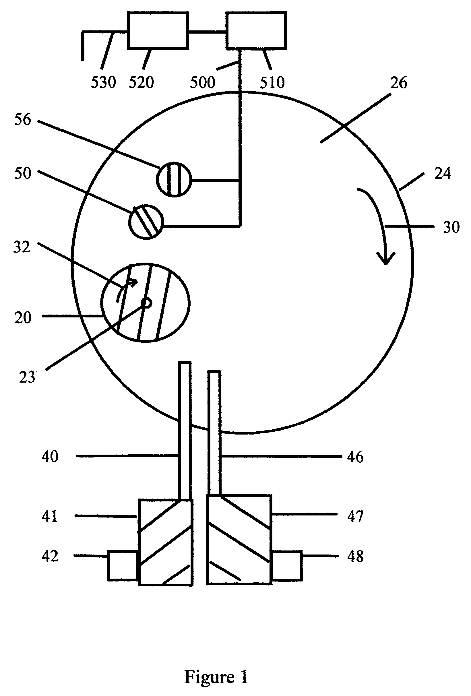
[0100]Using current cost of manufacture parameters along with a friction sensing method to evaluate and adjust the lubrication in a manner that adjustably controls the coefficient of friction in the operative finishing interface can be particularly effective at reducing unwanted surface defects such as microscratches and microchatter for some applications. This system is particularly preferred for planarizing or finishing with abrasive, more ...


PUM

PropertyMeasurementUnit
diameteraaaaaaaaaa
diameteraaaaaaaaaa
thickaaaaaaaaaa

Abstract

An apparatus for planarizing is disclosed. A method of planarizing is disclosed. Methods of planarizing using frictional planarizing, chemical planarizing, tribochemical planarizing, CVD planarizing, and electrochemical planarizing and combinations thereof are disclosed. A planarizing chamber can be used. New methods of control are planarizing disclosed. The new planarizing methods and apparatus, can help improve yield and lower the cost of manufacture for planarizing of workpieces having extremely close tolerances such as semiconductor wafers. Cost of manufacture parameters are used for control. Methods to determine preferred changes to process control parameters are disclosed. Cost of manufacture models can be used and are disclosed. Process models can be used and are disclosed. A method to use business calculations combined with physical measurements to improve control is discussed. Use of business calculations to change the cost of finishing semiconductor wafers is discussed. The method can help cost of manufacture forecasting for pre-ramp-up, ramp-up, and commercial manufacture. Activity based accounting can be preferred for some applications. Planarizing fluids are preferred. Reactive planarizing aids are preferred. Electro-planarizing for adding and removing material is disclosed. New methods and new apparatus for non-steady state planarizing control are disclosed.

Description

CROSS REFERENCE TO RELATED APPLICATIONS[0001]This application claims benefit of Provisional Application Ser. No. 60 / 127,393 filed on Apr. 1, 1999 entitled “Control of semiconductor wafer finishing”; Provisional Application Ser. No. 60 / 128,278 filed on Apr. 8, 1999 entitled “Improved semiconductor wafer finishing control”, Provisional Application Ser. No. 60 / 128,281 filed on Apr. 8, 1999 entitled “Semiconductor wafer finishing with partial organic boundary lubricant”, Provisional Application Ser. No. 60 / 336,448 filed on Oct. 29, 2001 entitled “Wafer finishing control”, Provisional Application Ser. No. 60 / 332,002 filed on Nov. 23, 2001 entitled “Wafer refining control”, and Provisional Application Ser. No. 60 / 393,212 filed on Jul. 7, 2002 entitled “Wafer refining”. This application claims benefit of Utility patent application Ser. No. 09 / 435,181 filed on Nov. 5, 1999 entitled “In situ friction detector method for finishing semiconductor wafers” which is now U.S. Pat. No. 6,283,289, Ut...

Claims


Application Information

Patent Timeline
Patent Type & Authority Patents(United States)
IPC IPC(8): B24B49/00B24B51/00B24B37/04
CPCB24B37/042B24B49/00G05B19/41875G05B2219/45232G05B2219/32216Y02P90/02Y02P90/80
Inventor MOLNAR, CHARLES J.
Owner SEMCON TECH
Why Eureka
Try Eureka