
Sensor circuit and method of producing it

a sensor circuit and sensor technology, applied in the field of sensor circuits, can solve the problems of yield loss, sensitivity differences between hall elements of such monolithically integrated hall sensors, etc., and achieve the effects of low requirements for production technology stability, low chip area consumption, and high precision

Inactive Publication Date: 2006-05-02
INFINEON TECH AG
View PDF22 Cites 5 Cited by
  • Summary
  • Abstract
  • Description
  • Claims
  • Application Information

AI Technical Summary

Benefits of technology

[0008]It is the object of the present invention to provide a sensor circuit and a method of producing it, having a high precision with a low chip area consumption and low requirements regarding the stability of the production technology.
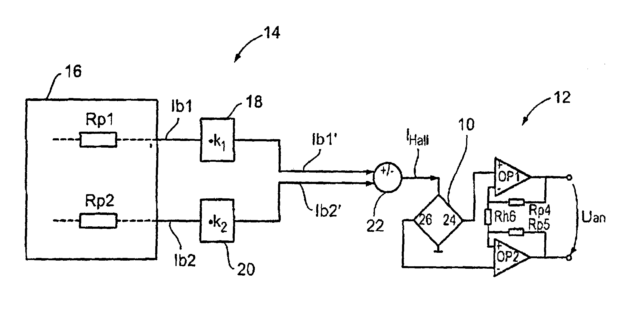
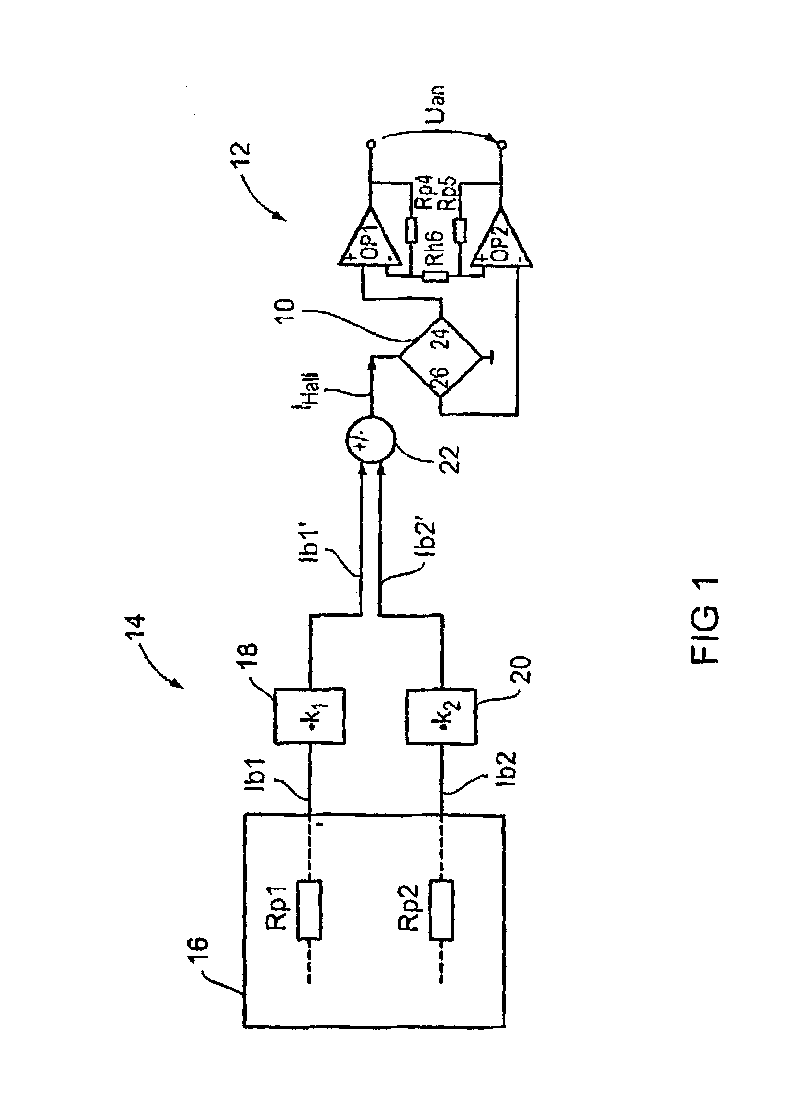
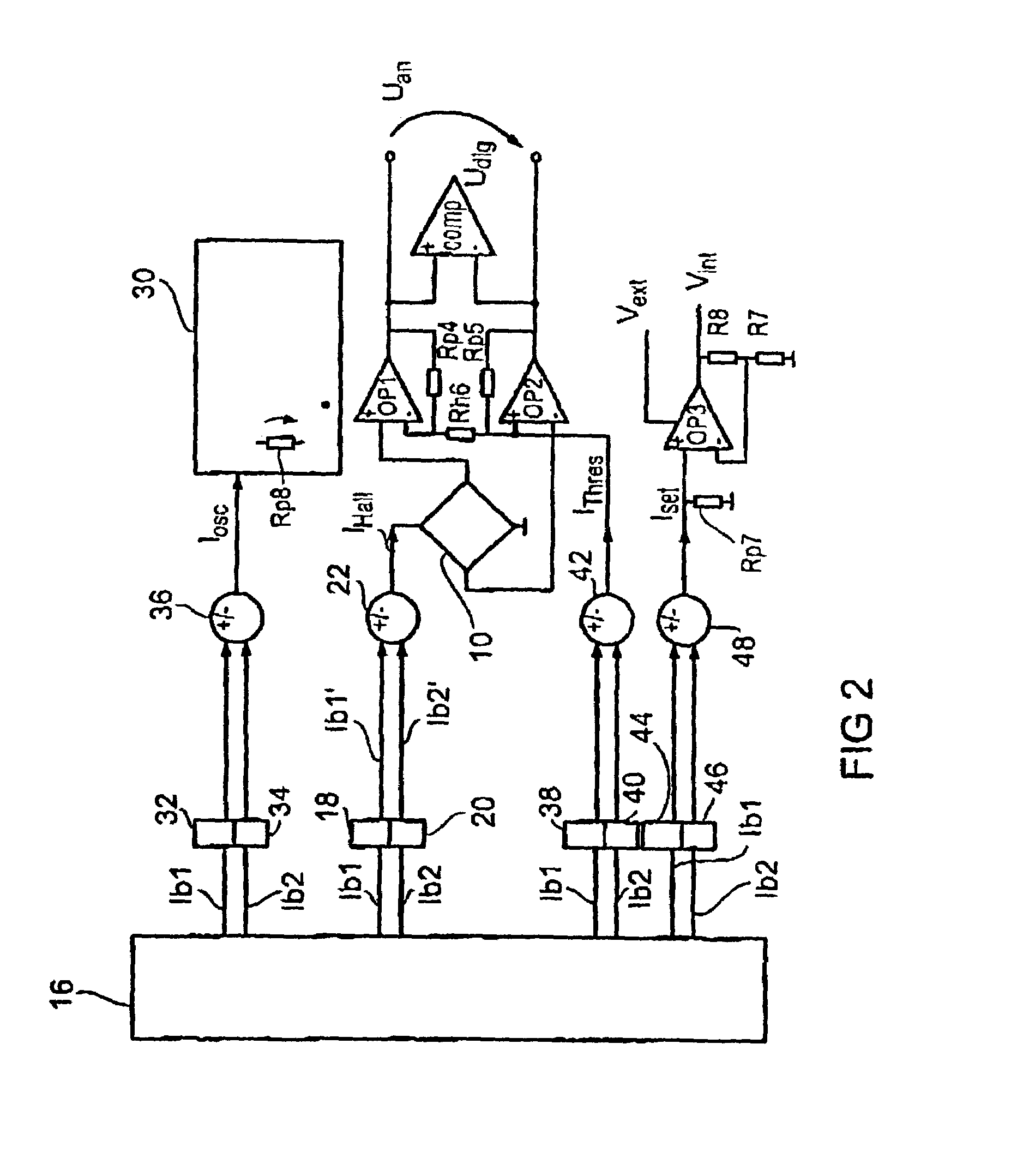
[0021]In preferred embodiments of the inventive sensor circuit currents are derived from the band gap circuit representing the current source by a sum or difference formation, the currents producing voltages across the reverse feedback resistors of the amplifier circuit or other poly-resistors, wherein the voltages must be overcome by the applying magnetic field and thus the sensor voltage generated in order to have a comparator switch. Thus, the same band gap circuit can be used for a threshold production for magnetic switching points, wherein the advantage lies in the fixed dimensionability of the quantity and the temperature dependency of these voltages serving as switching thresholds. Thus, the magnetic switching points can be set precisely for switching the sensor.
[0025]The present invention provides a sensor circuit which can do with a very small chip area and has thus a small-area characteristic. In addition, the present invention enables a very high yield by self-compensation and robustness as regards technology variations, i.e. only low requirements are made to the stability of the production technology. By the multiple usage of the only band gap circuit, a drastically reduced chip area results since not three or four band gap circuits must be used, as has been the case before. According to the invention, area-intense and leakage current susceptible Hall resistors in the bias system, as are, for example, used according to EP 0525235 B1, can be dispensed with so that the present invention enables precise output voltages or switching points even at high temperatures. Finally, the present invention provides a high-precision sensor circuit without the necessity of equalizing measures on the wafer or in the package.

Problems solved by technology

The Hall elements of such monolithically integrated Hall sensors have sensitivity differences due to technology and temperature.
Finally, the Hall elements can be measured, wherein such Hall elements not satisfying a predetermined specification are sorted out, which has the consequence of a yield loss.
It is a disadvantage of the bias system of EP0525235B1 described above, which bases on resistors formed like the Hall element that such resistors have a large area and large leakage currents at high temperatures.

Method used


Image

  • Sensor circuit and method of producing it
  • Sensor circuit and method of producing it
  • Sensor circuit and method of producing it

Examples


Embodiment Construction

[0033]Although preferred embodiments of the present invention will be detailed subsequently referring to Hall sensors, it is obvious that the present invention can be applied to other sensor elements producing an output voltage to be amplified, in particular to other magnetic field sensor elements the output voltage of which depends on a magnetic field applying. The set up of such sensors, such as, for example, Hall sensor elements, magnetoresistive sensor elements and giant magnetoresistive sensor elements, is well known to those skilled in the art and does not need to be explained further.

[0034]FIG. 1 shows an embodiment of a sensor circuit embodying the present invention. The sensor circuit includes a Hall element or Hall plate 10 the voltage tapping terminals of which are connected to an amplifier circuit 12 and the operating current terminals of which are connected between a current source 14 and ground. The Hall element thus can be formed in a well-known way by means of a dope...


PUM


Abstract

A sensor circuit includes a sensor element, a current source for supplying an operating current for the sensor element and an amplifier circuit for amplifying a sensor voltage produced by the sensor element when applying the operating current, wherein the amplifier circuit has a resistor influencing the amplification of it. The resistor of the amplifier current and the sensor element are formed equally as regards technology so that variations, due to technology, of the sensor sensitivity of the sensor element are counteracted by an amplification factor of the amplifier circuit changing in the opposite way.

Description

BACKGROUND OF THE INVENTION[0001]1. Field of the Invention[0002]The present invention relates to a sensor circuit and to a method of producing it and, in particular, to a magnetic sensor circuit having a sensor element the output signal of which depends on an external magnetic field, a current source for providing an operating current for the sensor element and an amplifier circuit for amplifying a sensor voltage produced by the sensor element.[0003]2. Description of the Related Art[0004]Monolithically integrated magnetic sensors, such as, for example Hall sensors, magnetoresistive sensors and so-called giant magnetoresistive sensors, are commercially available and are increasingly utilized, apart from their actual usage as measuring devices for magnetic fields, where a contactless switching is to be effected. Such a field is, for example, revolution counting in the gear or tachometer area of motor vehicles. The Hall elements of such monolithically integrated Hall sensors have sensi...

Claims


Application Information

Patent Timeline
IPC IPC(8): G01R33/02G01D3/036G01D5/14G01D5/16G01D5/244H03F3/45
CPCG01D3/036G01D5/145G01D5/2448H03F3/45475G01D5/24428H03F2200/261
Inventor MOTZ, MARIO
Owner INFINEON TECH AG
Learn More