Liquid crystal display device having high light utilization efficiency

a technology of liquid crystal display and light utilization efficiency, which is applied in the direction of identification means, instruments, optics, etc., can solve the problems of reducing light utilization efficiency, and achieve the effects of reducing the aperture rate of pixels, high light utilization efficiency, and sufficient supplementary capacitan

Inactive Publication Date: 2006-05-02
SHARP KK
View PDF12 Cites 27 Cited by
  • Summary
  • Abstract
  • Description
  • Claims
  • Application Information

AI Technical Summary

Benefits of technology

[0009]Accordingly, the object of the present invention is to provide a liquid crystal display device that can obtain high light utilization efficiency and a s

Problems solved by technology

Therefore, depending on the film forming conditions, the films become the films for absorbing the light in the short wavelength region, while reflection tends to occur on the interfaces of the pixel elect

Method used


Image

  • Liquid crystal display device having high light utilization efficiency
  • Liquid crystal display device having high light utilization efficiency
  • Liquid crystal display device having high light utilization efficiency

Examples


Embodiment Construction

[0036]The liquid crystal display device of the present invention will be described below on the basis of the embodiment thereof shown in the drawings.

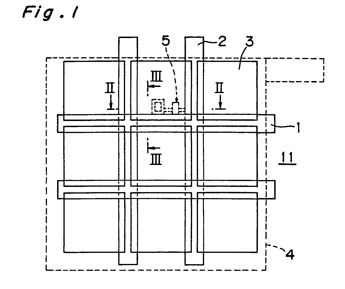
[0037]FIG. 1 is a schematic plan view of the thin film transistor array substrate of a liquid crystal display device according to one embodiment of the present invention, showing a planar type thin film transistor array of the thin film transistor array substrate that employs polysilicon.

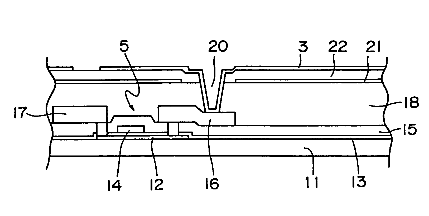
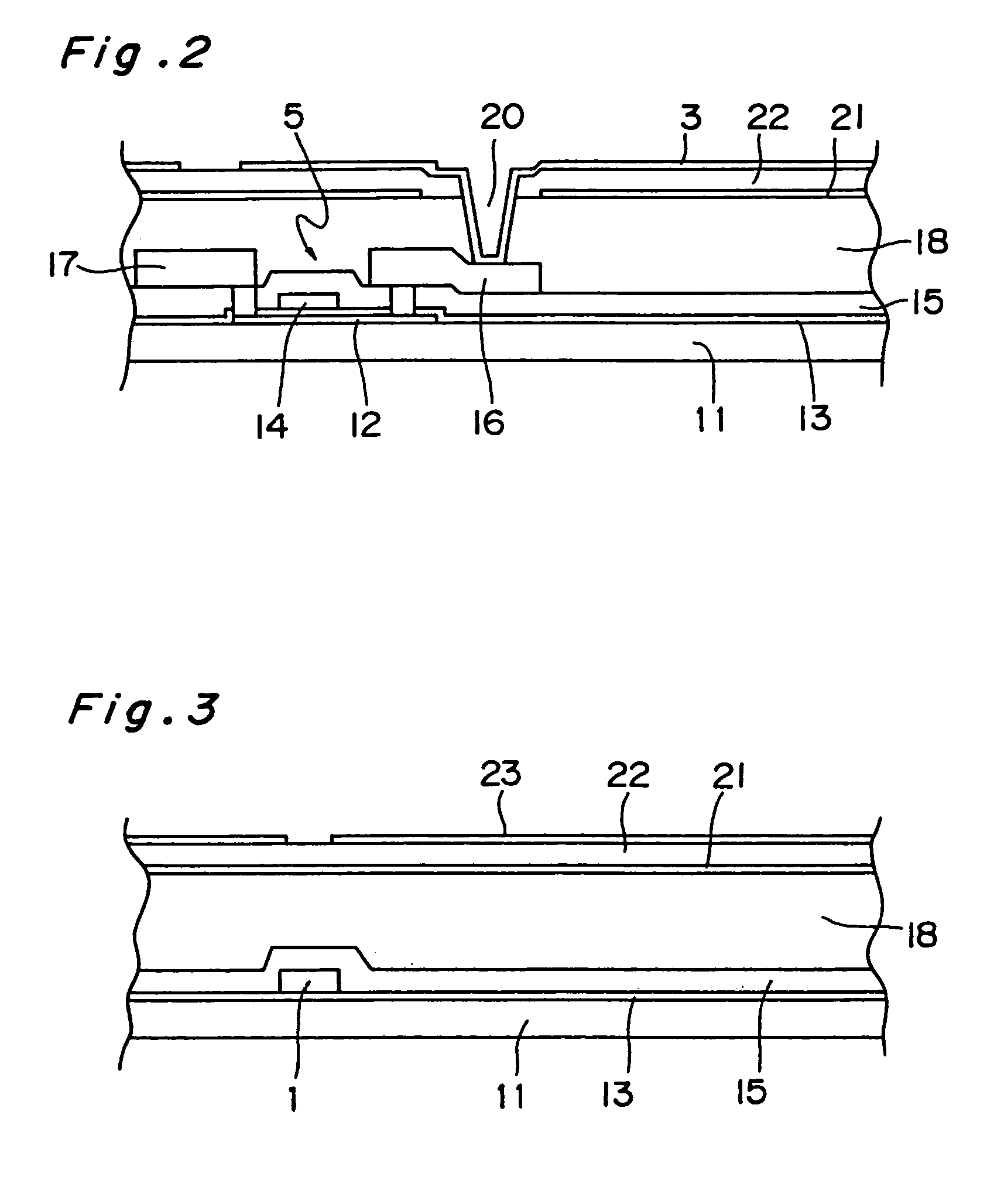
[0038]As shown in FIG. 1, according to the thin film transistor array substrate, a plurality of gate bus lines 1, a plurality of signal lines 2 formed perpendicularly to the plurality of gate bus lines 1 and a plurality of pixel electrodes 3 arranged so that their edges overlap the gate bus lines 1 and the signal lines 2 are formed on a transparent substrate 11. The transparent substrate 11 is made of aluminoborosilicate glass having a high heat resistance. Although FIG. 1 shows 3×3 pixel electrodes for the sake of providing a clear view, the number of...


PUM


Abstract

There is provided a liquid crystal display device that can obtain a high light utilization efficiency and a sufficient supplementary capacitance without reducing an aperture rate of pixels and is able to attain higher resolution. A silicon nitride film 22 that serves as a supplementary capacitance use transparent insulating film is formed under a pixel electrode 3. A common electrode 21 that is made of ITO and is connected to a potential common to an opposite electrode is formed under the silicon nitride film 22. The pixel electrode 3, the silicon nitride film 22 and the common electrode 21 constitute the supplementary capacitance, and the pixel electrode 3, the silicon nitride film 22 and the common electrode 21 are each made to have a film thickness such that a transmittance is increased by interference at a specified wavelength.

Description

BACKGROUND OF THE INVENTION[0001]The present invention relates to a liquid crystal display device that employs a thin film transistor array substrate provided with a supplementary capacitance for each pixel.[0002]In recent years, as a thin type light-weight display having a low power consumption, an active matrix type liquid crystal display device in which each pixel electrode is controlled by a semiconductor element such as a thin film transistor provided for each pixel electrode has attracted a great deal of attention among, in particular, liquid crystal display devices, since the device can obtain an excellent resolution and a vivid image. Reference will be made below to the active matrix type liquid crystal display device.[0003]As a semiconductor element for use in the conventional active matrix type liquid crystal display device, a thin film transistor constructed of an amorphous silicon thin film has been known, and a great many active matrix type liquid crystal display device...

Claims


Application Information

Patent Timeline
IPC IPC(8): G02F1/1343G02F1/136G02F1/1333G09F9/30G02F1/1335G02F1/1362G02F1/1365G02F1/1368H01L21/336H01L29/786
CPCG02F1/133502G02F1/136213G02F1/136227G02F1/136
Inventor KATSUYA, YOKO
Owner SHARP KK
Why Eureka
Try Eureka