

Optical wavelength converting apparatus, and optical wavelength converting method
a technology of optical wavelength and converting apparatus, which is applied in the direction of light demodulation, instrumentation, laser details, etc., can solve the problems of high conversion efficiency of sum frequency light, unstable output, and difficult phase-match longitudinal modes of those two resonators with the sum frequency light, etc., and achieve high conversion efficiency and high-speed modulation
- Summary
- Abstract
- Description
- Claims
- Application Information
AI Technical Summary
Benefits of technology
Problems solved by technology
Method used
Image

Examples
first embodiment
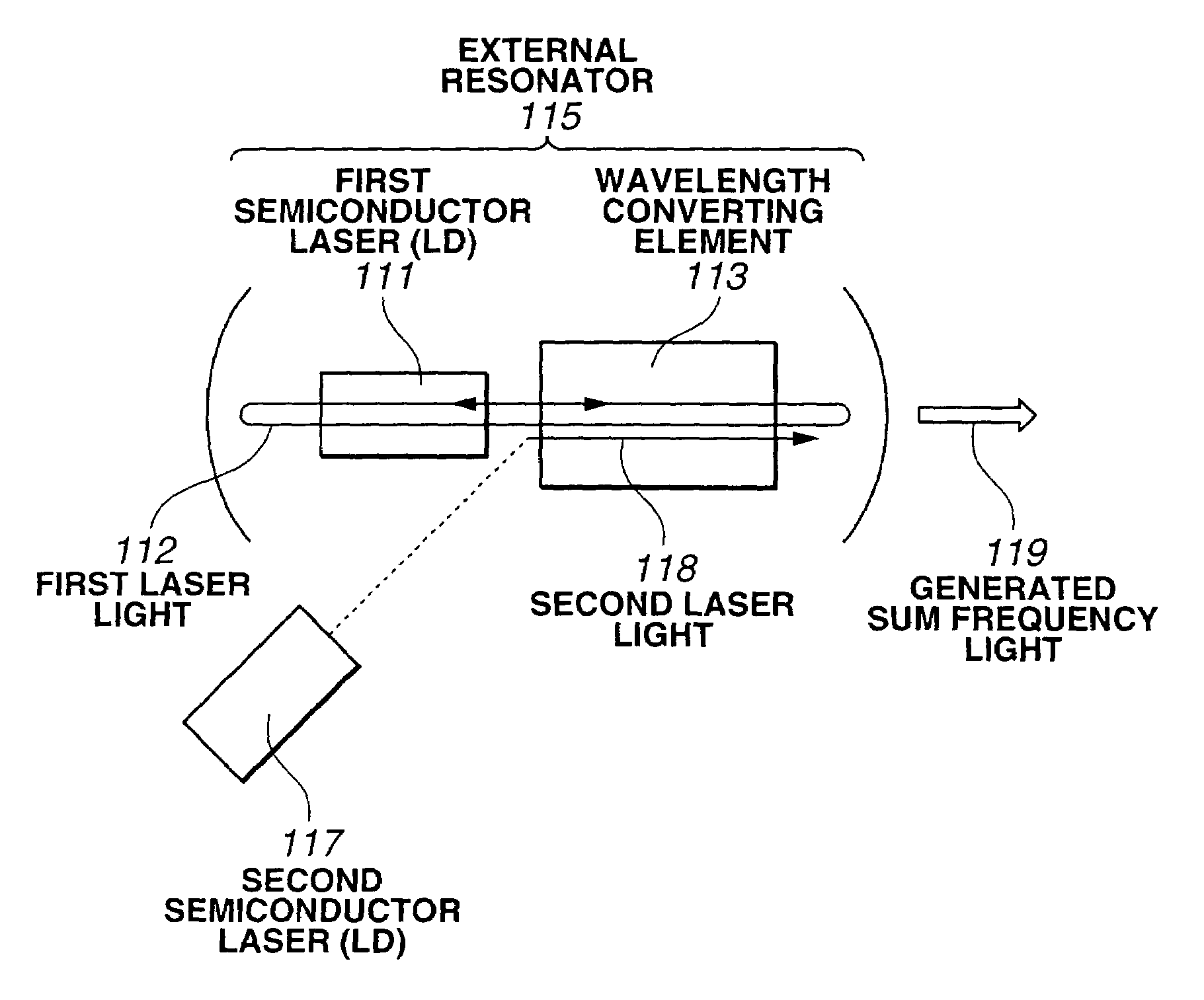
[0034]FIG. 1 is a schematic view illustrating the optical wavelength converting apparatus of the In FIG. 1, there are arranged a first semiconductor laser (LD) 111, a second semiconductor laser (LD) 112, and a wavelength converting element 113 (for example, a KTP crystal of nonlinear optical material). An external resonator 115 is constructed by the first LD 111, the wavelength converting element 113, and a pair of reflective surfaces (not shown). In the external resonator 115, the first LD 111 is disposed such that first laser light 112 emitted by the first LD 111 can reciprocate between a pair of reflective surfaces, and can be put under a resonant condition.
[0035]The second LD 117 is disposed outside the external resonator 115. Second laser light 118 emitted by the second LD 117 is guided into the wavelength converting element 113 to generate sum frequency light 119. In the first embodiment, the second laser light 118 emitted by the second LD 117 is introduced into the wavelengt...
second embodiment
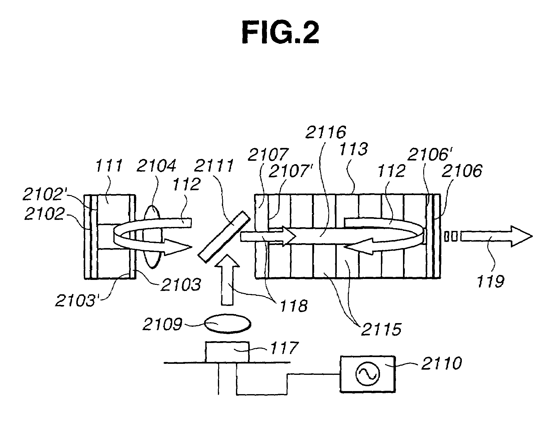
[0049]FIG. 2 illustrates the optical wavelength converting apparatus of the In FIG. 2, reference numeral 2115 represents a periodically domain-inverted structure. Reference numerals 2107 and 2103 represent dielectric multi-layers, respectively. Reference numerals 2102 and 2106 represent dielectric multi-layers acting as reflective surface mirrors, respectively. Reference numerals 2104 and 2109 represent condenser lenses, respectively. Reference numeral 2111 represents a beam splitter. Reference numeral 2110 represents a driving circuit for driving the second semiconductor laser 117.
[0050]Light from the first semiconductor laser 111 travels in a reciprocatory manner between the mirror 2102 formed on an end face 2102′ of the first semiconductor laser 111 opposite to its light emitting end face 2103′ and the mirror 2106 formed on an end face 2106′ of the wavelength converting element 113 opposite to its light input side. The light from the first semiconductor laser 111 is thus put und...
third embodiment
[0069]FIG. 7 illustrates the optical wavelength converting apparatus of the In FIG. 7, reference numeral 503 represents a mirror. The mirror 503 is arranged away from the wavelength converting element 113. Reference numeral 505 represents a dielectric multi-layer. The mirror 503 is preferably a concave mirror for light emerging from the wavelength converting element 113. In such a structure, even when light from the wavelength converting element 113 is thick or divergent, the light can be thinned and returned to the wavelength converting element by reflection at the concave mirror 503. Where the mirror 503 has a curved surface concave against the wavelength converting element 113, the waveguide can be omitted in the wavelength converting element.
[0070]The dielectric multi-layer 505 is disposed at the end portion of the wavelength converting element according to necessity. The dielectric multi-layer 505 is antireflective to light from the first semiconductor laser 111.
[0071]In more ...
PUM
| Property | Measurement | Unit |
|---|---|---|
| wavelength | aaaaa | aaaaa |
| wavelength | aaaaa | aaaaa |
| wavelength | aaaaa | aaaaa |
Abstract
Description
Claims
Application Information