

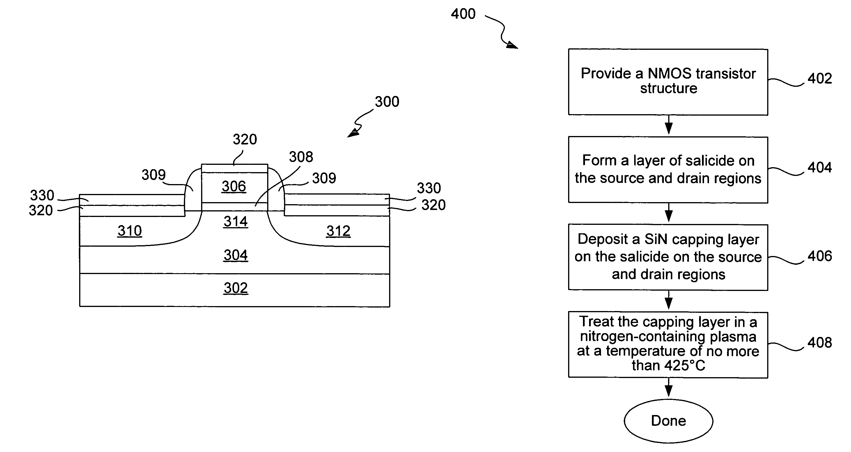
Strained transistor architecture and method
a transistor and strain technology, applied in the field of strain transistor architecture for nmos devices, can solve the problems of reducing processing time, and achieve the effects of enhancing the performance of the resulting transistor, preserving material quality, and avoiding adverse effects on the efficiency of the transistor fabrication process
- Summary
- Abstract
- Description
- Claims
- Application Information
AI Technical Summary
Benefits of technology
Problems solved by technology
Method used
Image

Examples
example
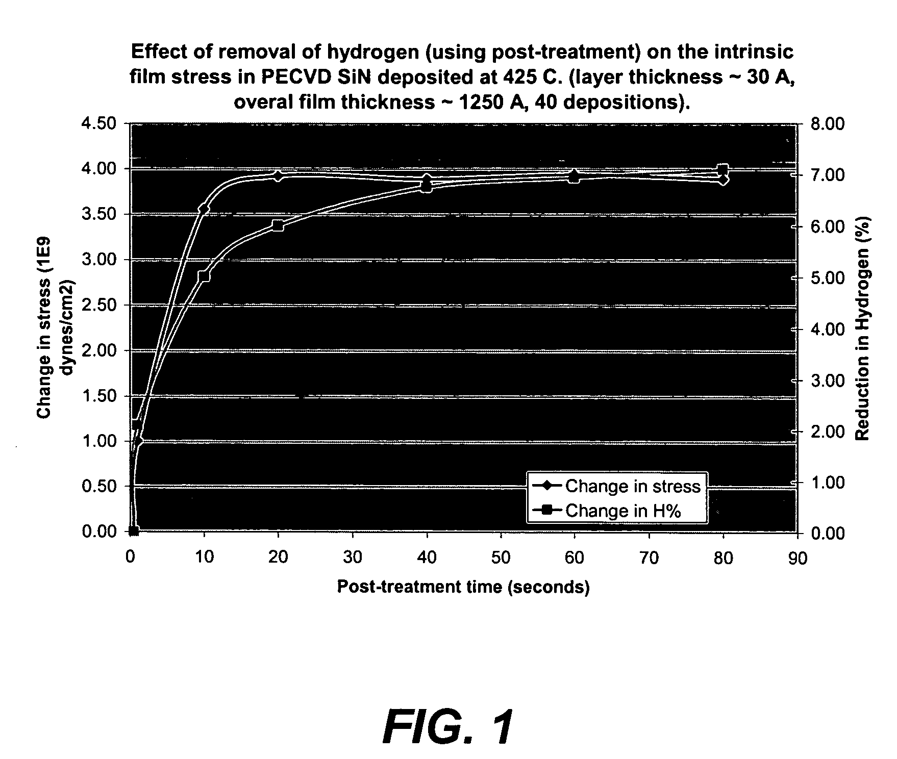
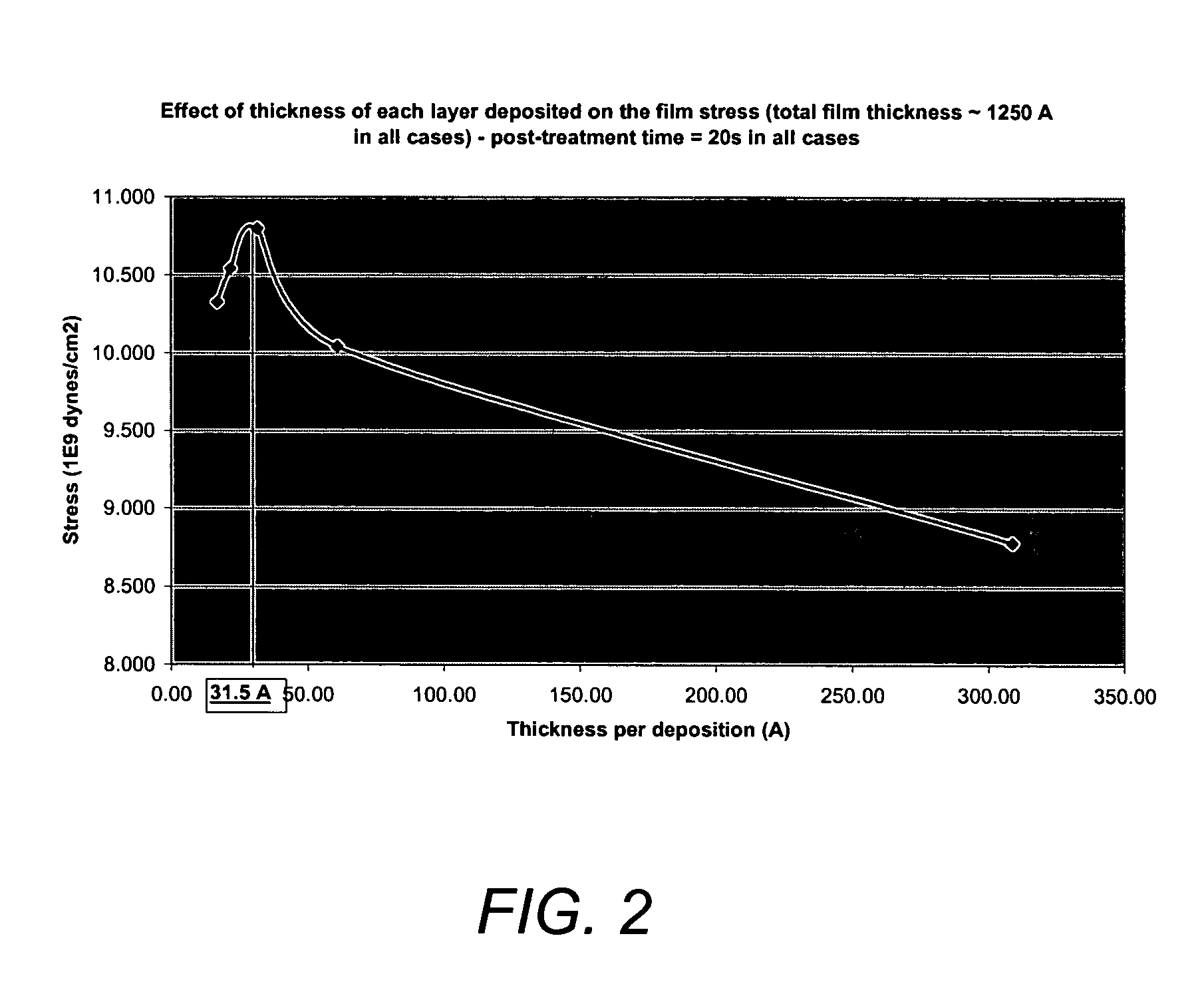
[0046]The following example is provided to further illustrate aspects and advantages of the present invention. This example is provided to exemplify and more clearly illustrate aspects of the present invention and is in no way intended to be limiting.
[0047]A SiN capping layer film was deposited over 10, 25 or 40 depositions (Station Deposition Time (SDT) reduced accordingly to get the same overall film thickness of 1250 Å), rather than the conventional 4 depositions. Each deposition was followed by a plasma anneal treatment using the same flows of N2 and NH3 and the same HF power as in the deposition process, but shutting off the SiH4 flow. The 40-deposition process, with a post-treatment of 20s after every deposition was found to increase the stress from 8 E9 to 1.20 E10 dynes / cm2, while the 10 and 25 deposition processes with the same 20s post-treatment after every deposition provided stresses of 9.2 E9 and 10.5 E9 dynes / cm2, respectively. This experiment demonstrates that reducin...
PUM
 Abstract
Description
Claims
Application Information