Semiconductor light emitting device and method for producing the same

a technology of semiconductor laser and light emitting device, which is applied in the direction of lasers, semiconductor laser structure details, semiconductor lasers, etc., can solve the problems of increased cost of semiconductor laser devices and variability in the production yield of semiconductor laser devices, and achieve stable oscillation threshold current, improved reliability, and suppression of light by impurities

Inactive Publication Date: 2006-05-09
SHARP KK
View PDF21 Cites 0 Cited by
  • Summary
  • Abstract
  • Description
  • Claims
  • Application Information

AI Technical Summary

Benefits of technology

[0021]According to a semiconductor light emitting device of the present invention, the interface between the semiconductor current confinement layer and the semiconductor etching stop layer and the interface between the semiconductor current confinement layer and the ridge structure each have an impurity content of less than 1×10¹⁷ / cm3. Therefore, absorption of light by the impurities is suppressed, the oscillation threshold current Ith is stable without being abnormally increased, the malfunction rate when continuously used for a long period of time is lowered, and the reliability is improved.
[0022]Thus, the invention described herein makes possible the advantages of providing a semiconductor light emitting device for suppressing the increase in the oscillation threshold current Ith and improving the reliability, and a method for producing the same.

Problems solved by technology

Depending on the process conditions, the oscillation threshold current Ith, which is a starting point of laser oscillation, may be increased, which causes variability in the production yield of the semiconductor laser devices.
This is a cause of the increased cost of semiconductor laser devices.

Method used


Image

  • Semiconductor light emitting device and method for producing the same
  • Semiconductor light emitting device and method for producing the same
  • Semiconductor light emitting device and method for producing the same

Examples


Embodiment Construction

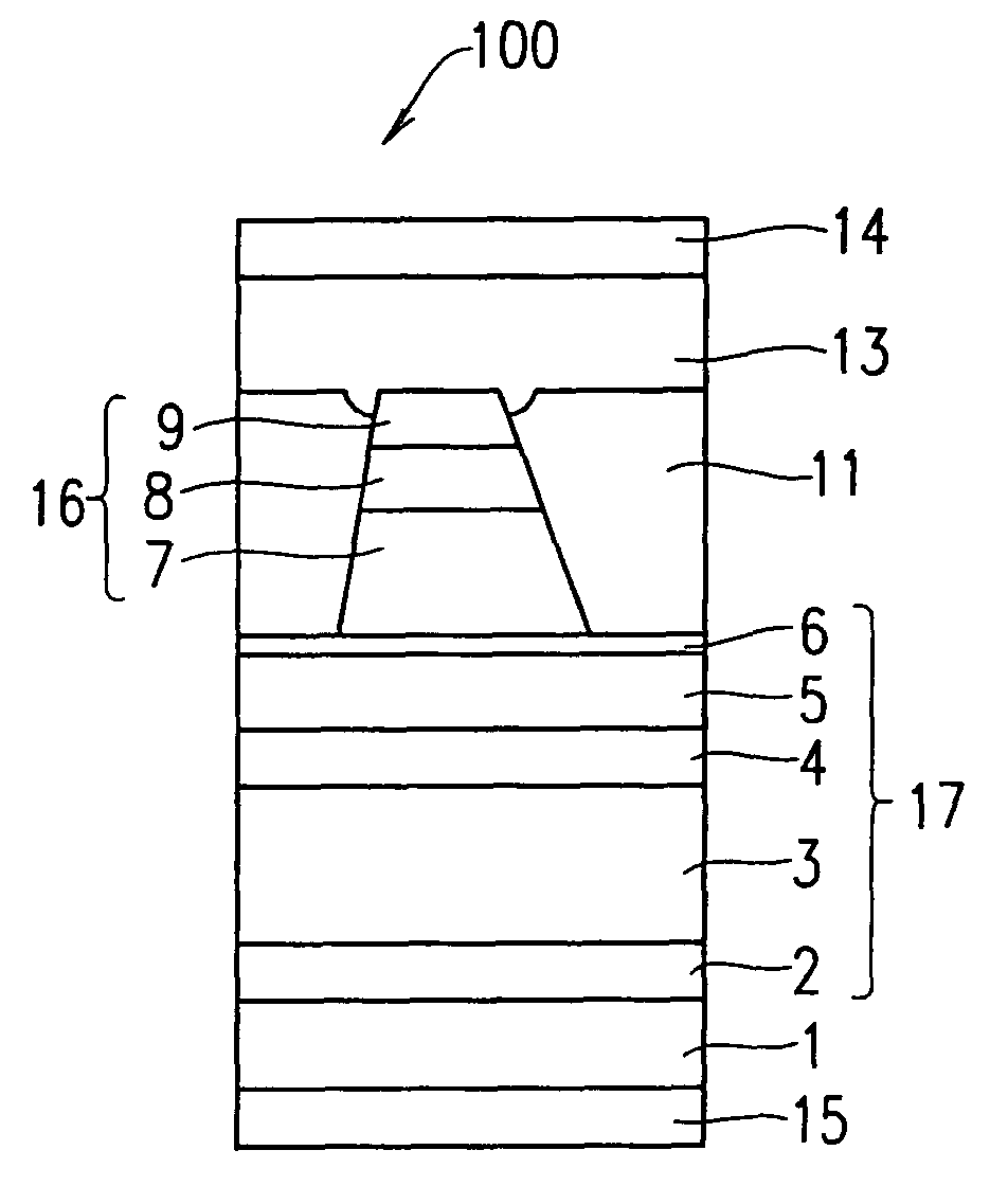
[0031]Samples of each layer of the semiconductor laser device 200 produced by the method shown in FIG. 5A through 5D were analyzed in terms of crystalline state and the like using a SIMS (secondary ion mass spectrometer) and the like. The following was found.

[0032]In a semiconductor laser device of a lot having an abnormally high oscillation threshold current Ith, the content of carbon-based impurities and oxygen-based impurities at the interface between the n-type AlInP current confinement layer 111 and the p-type GaInP etching stop layer 106 and the interface between the n-type AlInP current confinement layer 111 and the striped ridge structure 116 (more specifically, the re-growth interface area of the n-type AlInP current confinement layer 111) was confirmed to be higher than that of a semiconductor laser device of a lot having a normal oscillation threshold current Ith.

[0033]It was also confirmed that the content of the carbon-based impurities and oxygen-based impurities in the...


PUM


Abstract

A semiconductor light emitting device includes a semiconductor substrate; a stacked semiconductor structure formed on the semiconductor substrate; a striped ridge structure; and a semiconductor current confinement layer provided on a side surface of the striped ridge structure. The stacked semiconductor structure includes a first semiconductor clad layer, a semiconductor active layer, a second semiconductor clad layer, and a semiconductor etching stop layer. The striped ridge structure includes a third semiconductor clad layer, a semiconductor intermediate layer, and a semiconductor cap layer. The striped ridge structure is provided on the semiconductor etching stop layer. An interface between the semiconductor current confinement layer and the semiconductor etching stop layer and an interface between the semiconductor current confinement layer and the striped ridge structure each have a content of impurities of less than 1×10¹⁷/cm3.

Description

BACKGROUND OF THE INVENTION[0001]1. Field of the Invention[0002]The present invention relates to a semiconductor light emitting device used for an optical recording apparatus, an optical transmission apparatus or the like, and a method for producing the same.[0003]2. Description of the Related Art[0004]Recently, optical recording apparatuses and optical transmission apparatuses have been used in various apparatuses in information related fields. Semiconductor laser devices used as semiconductor light emitting devices in these optical recording apparatuses and optical transmission apparatuses have been required to have high performances in terms of speed, output and the like.[0005]As devices in information related fields are used more and more in households, the semiconductor laser devices used in these optical recording apparatuses and optical transmission apparatuses are required to be inexpensive. For example, semiconductor laser devices used in optical recording apparatuses, for ...

Claims


Application Information

Patent Timeline
Patent Type & Authority Patents(United States)
IPC IPC(8): H01L21/00H01L33/00B82Y20/00H01S5/02H01S5/20H01S5/22H01S5/223H01S5/323
CPCH01S5/22H01S5/32325H01S5/2231H01L33/145H01S5/209H01S5/2226H01S5/2201
Inventor TANI, KENTARO
Owner SHARP KK
Why Eureka
Try Eureka