Silicon-oxycarbide high index contrast, low-loss optical waveguides and integrated thermo-optic devices

a technology of optical waveguides and silicon carbide, which is applied in glass making apparatus, instruments, manufacturing tools, etc., can solve the problems of power consumption affecting the cost of optical systems, sioc films have a refractive index less than that of sio, and achieve low stress values

Inactive Publication Date: 2006-05-09
INFINERA CORP
View PDF53 Cites 36 Cited by
  • Summary
  • Abstract
  • Description
  • Claims
  • Application Information

AI Technical Summary

Benefits of technology

[0012]The present invention addresses the aforementioned issues to a great extent by providing an optical core element having a refractive index of between about 1.5 and 2.5 and having a dn/dT of between about 1×10⁻⁵/° C. and about 3×10⁻⁵/° C. By using a standard CVD (chemical vapor deposition) process such as PECVD (plasma-enhanced CVD), a stable and uniform SiOC film may be deposited having a film stress that is tunable from tensile to highly compressive and that can be optimized to have a low stress value of less than 100 MPa. When combined with an optical cladding such as SiO2, the SiOC optical core element can be used to form optical waveguides with refractive index contrasts as high as about 0.72 (72%).
[0013]In some embodiments, the silicon-oxycarbide optical waveguides and thermooptic devices include a substrate or wafer that may contain preformed optical and electronic devices. A first cladding layer having a first refractive index is positioned on the substrate or wafer. A first core layer comprising silicon, oxygen, and carbon and having a core refractive index is formed on the first cladding layer by chemical vapor deposition using at least two precursors: one inorganic silicon precursor gas and at least one second precursor gas comprising carbon and oxygen. Alternatively, precursors can be selected such that there are...

Problems solved by technology

A primary factor contributing to the overall performance of an integrated optical circuit containing thermooptic devices is power consumption.
Power consumption affects the cost of optical systems through footprint, t...

Method used


Image

  • Silicon-oxycarbide high index contrast, low-loss optical waveguides and integrated thermo-optic devices
  • Silicon-oxycarbide high index contrast, low-loss optical waveguides and integrated thermo-optic devices
  • Silicon-oxycarbide high index contrast, low-loss optical waveguides and integrated thermo-optic devices

Examples


Embodiment Construction

[0017]In the following detailed description, a plurality of specific details, such as precursors and refractive index contrasts are set forth in order to provide a thorough understanding of the present invention. The details discussed in connection with the preferred embodiments should not be understood to limit the present invention. Furthermore, for ease of understanding, certain method steps are delineated as separate steps; however, these steps should not be construed as necessarily distinct nor order dependent in their performance.

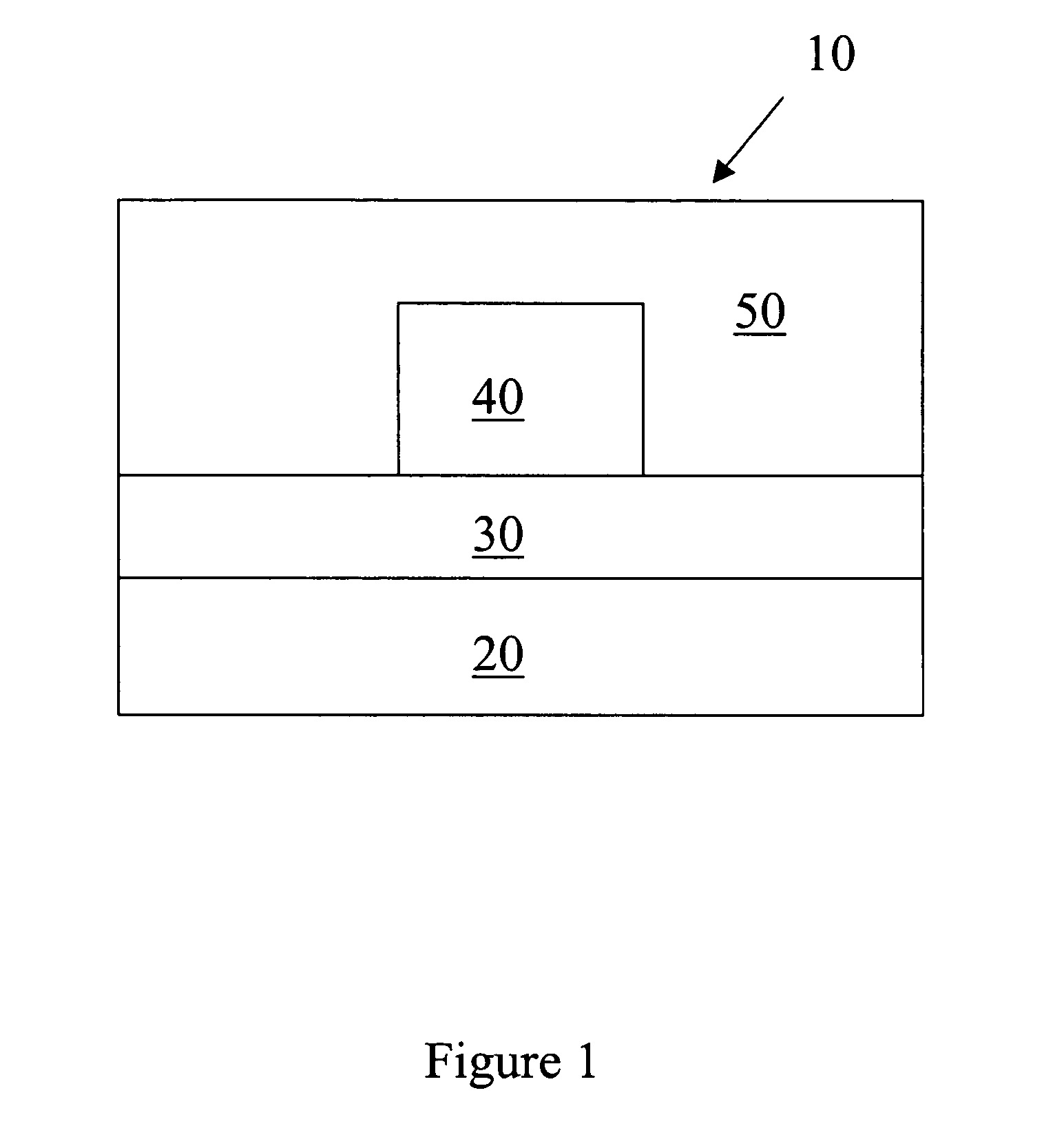
[0018]Optical waveguides are the fundamental building block of integrated optical devices and circuits. The expression “integrated optical circuits” includes a combination of optically transparent elongated structures for guiding, manipulating, or transforming optical signals that are formed on a common substrate or chip of monolithic or hybrid construction. The substrate can include electrical, optical, and optoelectronic devices and circuits. The tr...


PUM

PropertyMeasurementUnit
Thicknessaaaaaaaaaa
Thicknessaaaaaaaaaa
Widthaaaaaaaaaa

Abstract

Silicon-oxycarbide optical waveguides and thermooptic devices include a substrate and a first cladding layer having a first refractive index positioned over a substrate. A first core layer comprising silicon, oxygen, and carbon and having a core refractive index is formed on the first cladding layer by chemical vapor deposition using at least two precursors: one inorganic silicon precursor gas and at least one second precursor gas comprising carbon and oxygen. Alternatively, at least three precursors can be used: one inorganic silicon precursor gas, a second precursor comprising carbon, and a third precursor comprising oxygen. The core layer is lithographically patterned to define waveguide elements. A second cladding layer having a second cladding refractive index is formed to surround the optical core waveguiding element of the first core layer.

Description

[0001]This is a continuation-in-part of U.S. patent application Ser. No. 10 / 465,881 filed Jun. 20, 2003, now U.S. Pat. No. 6,771,868, which is a continuation of U.S. patent application Ser. No. 09 / 944,207 filed Sep. 4, 2001, now U.S. Pat. No. 6,614,977 which claims priority from U.S. Provisional Application Ser. No. 60 / 304,811 filed Jul. 12, 2001. The entirety of these applications is incorporated herein by reference.BACKGROUND OF THE INVENTION[0002]1. Field of the Invention[0003]This invention pertains to integrated optical circuits with optical waveguides having high index contrast and low optical loss for passive optical devices, thermooptic devices, and integrated optical circuits. More particularly, the invention pertains to the chemical vapor deposition of silicon-oxycarbide optical films and the formation of optical core elements and cladding layers to form optical waveguides and integrated thermooptic devices.[0004]2. Description of the Related Art[0005]Long haul, metropolit...

Claims


Application Information

Patent Timeline
IPC IPC(8): G02B6/00C03B37/022C03B37/023G02B6/10C03C17/34C23C16/30C23C16/40G02B6/12G02B6/132
CPCC03C4/0042C03C17/3435C03C17/3482C23C16/308C23C16/401G02B6/132C03C2218/152G02B2006/121G02B2006/12097C03C2218/33
Inventor JOHNSON, FREDERICK G.KING, OLIVER S.GILL, DAVID M.DAVIDSON, TIMOTHY J.BERK, WARREN P.
Owner INFINERA CORP
Why Eureka
Try Eureka