Delay locked loop and its control method

a delay model and control method technology, applied in pulse manipulation, pulse technique, instruments, etc., can solve the problems of large power consumption, large size of delay model units and phase detectors in each of the two feed-back loops, and achieve the effect of small siz

Inactive Publication Date: 2006-05-16
SK HYNIX INC
View PDF14 Cites 50 Cited by
  • Summary
  • Abstract
  • Description
  • Claims
  • Application Information

AI Technical Summary

Benefits of technology

[0033]It is, therefore, an object of the present invention to provide a DLL and a method for synchronizing an internal clock signal with an external clock signal and for correcting a duty ratio of the internal clock signal consuming low power and having a small size.

Problems solved by technology

However, a phase mixer, a delay model unit and a phase detector included in each of the two feed-back loops have a large size and consume much power.
Therefore, since the conventional DLL includes two feed-back loops, a size of the conventional DLL is increased and a power consumption of the conventional DLL is also increased.
Therefore, the conventional DLL may not be suitable to a small sized and low power consumed semiconductor memory device.
However, due to some variations such as a manufacturing process, a voltage and a temperature, a delay amount of one of the two feed-back loops may be different from that of the other.

Method used


Image

  • Delay locked loop and its control method
  • Delay locked loop and its control method
  • Delay locked loop and its control method

Examples


first embodiment

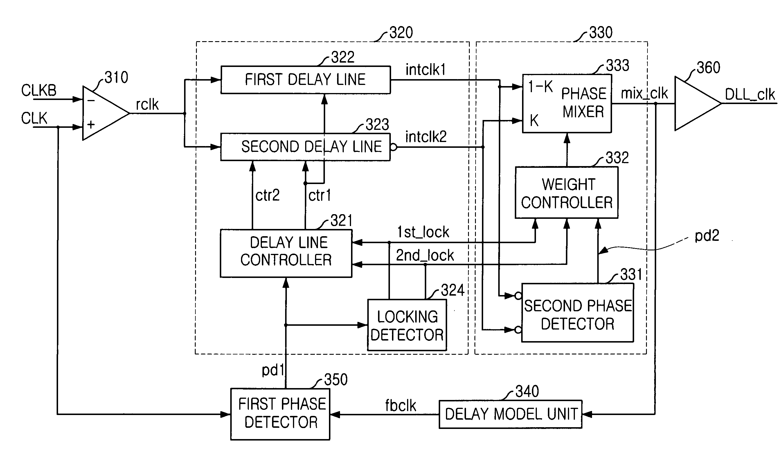
[0049]FIG. 3 is a block diagram showing a DLL in accordance with the present invention.

[0050]As shown, the DLL includes a first clock buffer 310, a second clock buffer 360, a delay line unit 320, a duty error control unit 330, a delay model unit 340 and a first phase detector 350.

[0051]The first clock buffer 310 receives an external clock signal CLK and its inverted signal, namely an external clock bar signal CLKB to output a rising edge clock signal rclk by buffering the external clock signal CLK and the external clock bar signal CLKB.

[0052]The delay line unit 320 receives the rising edge clock signal rclk and a first comparison signal pd1 to output a first delayed internal clock signal intclk1, a second delayed internal clock signal intclk2, a first delay locking signal 1st_lock and a second delay locking signal 2nd_lock.

[0053]The delay line unit 320 includes a first delay line 322, a second delay line 323, a delay line controller 321 and a locking detector 324.

[0054]The delay lin...

second embodiment

[0110]FIG. 9 is a block diagram showing a DLL in accordance with the present invention.

[0111]As shown, the DLL includes a first clock buffer 910, a second clock buffer 920, a third clock buffer 970, a delay line unit 930, a duty error control unit 940, a delay model unit 950 and a first phase detector 960.

[0112]The first clock buffer 910 receives an external clock signal CLK through a non-inverting terminal and its inverted signal, namely an external clock bar signal CLKB through an inverting terminal in order to output a first rising edge clock signal rclk1 by buffering the external clock signal CLK and the external clock bar signal CLKB.

[0113]The second clock buffer 920 receives an external clock signal CLK through an inverting terminal and the external clock bar signal CLKB through a non-inverting terminal in order to output a second rising edge clock signal rclk2 by buffering the external clock signal CLK and the external clock bar signal CLKB.

[0114]The delay line unit 930 recei...

third embodiment

[0129]FIG. 10 is a block diagram showing a DLL in accordance with the present invention.

[0130]As shown, the DLL includes a first clock buffer 1010, a second clock buffer 1050, a delay line unit 1020, a duty error control unit 1030, a delay model unit 1040 and a first phase detector 1050.

[0131]The first clock buffer 1010 receives an external clock signal CLK and its inverted signal, namely an external clock bar signal CLKB to output a rising edge clock signal rclk by buffering the external clock signal CLK and the external clock bar signal CLKB.

[0132]The delay line unit 1020 receives the rising edge clock signal rclk and a first comparison signal pd1 in order to output a first delayed internal clock signal intclk1, a second delayed internal clock signal intclk2, a first delay locking signal 1st_lock and a second delay locking signal 2nd_lock.

[0133]The delay line unit 1020 includes a first delay line 1022, a second delay line 1023, a delay line controller 1021 and a locking detector 1...


PUM


Abstract

A delay locked loop (DLL) capable of correcting a duty ratio of a clock signal including: a clock buffer which receives an external clock signal for outputting a rising edge clock signal; a delay unit for delaying the rising edge clock signal based on a first comparison signal in order to generate a first internal clock signal, a second internal clock signal, a first delay locking signal and a second delay locking signal; a duty correction unit for receiving the first and the second internal clock signals and the first and the second delay locking signals and generating a delay locked clock signal by correcting a duty cycle of the external clock signal; and a clock feed-back unit for receiving the delay locked clock signal and the external clock signal in order to generate the first comparison signal.

Description

FIELD OF INVENTION[0001]The present invention relates to a delay locked loop (DLL); and, more particularly, to an apparatus and a method for compensating a skew between an internal clock signal and an external clock signal and for correcting a duty error.DESCRIPTION OF PRIOR ART[0002]Generally, a delay locked loop (DLL) is used for a synchronous semiconductor memory device in order to synchronize an internal clock signal with an external clock signal. In the synchronous semiconductor memory device, data access operations such as a read operation and a write operation are performed in synchronization with rising and falling edges of the external clock signal.[0003]Since there is a time delay while the external clock signal is inputted to the synchronous semiconductor memory device, the DLL is employed for synchronizing the internal clock signal with the external clock signal by compensating the time delay between the internal clock signal and the external clock signal.[0004]However, ...

Claims


Application Information

Patent Timeline
Patent Type & Authority Patents(United States)
IPC IPC(8): H03L7/06G11C11/407H03L7/08H03L7/081H03L7/087H03L7/095
CPCH03L7/0812H03L7/087H03L7/095H03L7/0816G11C11/407
Inventor KWAK, JONG-TAE
Owner SK HYNIX INC
Why Eureka
Try Eureka