Method for scalable architectures in stackable three-dimensional integrated circuits and electronics

a three-dimensional integrated circuit and scalable technology, applied in the direction of originals for photomechanical treatment, semiconductor/solid-state device details, instruments, etc., can solve the problems of small alleviation of design effort and masking costs associated with each die, the three-dimensional techniques described do not apply to digital logic or digital logic coupled with memories, and reduce power consumption. , to achieve the effect of increasing the stacking level

Inactive Publication Date: 2006-05-16
SUNG RAYMOND JIT HUNG +4
View PDF18 Cites 48 Cited by
  • Summary
  • Abstract
  • Description
  • Claims
  • Application Information

AI Technical Summary

Benefits of technology

[0025]The methods described enable scalable integrated circuit systems in which circuits on different die, in a vertical three-dimensional stack of dies, are identical. Only one mask set is required for the entire stack. The system scales directly as the level of stacking is increased while incurring no extra design effort as the stack height increases.

Problems solved by technology

While extending these circuits to three-dimensions has the effect of reducing global interconnect length, they do little to alleviate the design effort and mask costs associated with each die.
Furthermore, the three-dimensional techniques described do not apply to digital logic or digital logic coupled with memories.
Reducing the stacking interval (distance between adjacent dies) in these technologies reduces wire lengths even further, resulting in reduced power consumption and increased logic speed.
However, self-heating effects, alignment issues and circuit yield impose limits on the stack height.

Method used


Image

  • Method for scalable architectures in stackable three-dimensional integrated circuits and electronics
  • Method for scalable architectures in stackable three-dimensional integrated circuits and electronics
  • Method for scalable architectures in stackable three-dimensional integrated circuits and electronics

Examples


Embodiment Construction

[0039]The preferred embodiments of the present invention are illustrated in FIGS. 1 through 6 of the drawings like numerals being used to refer to like and corresponding parts of the various drawings.

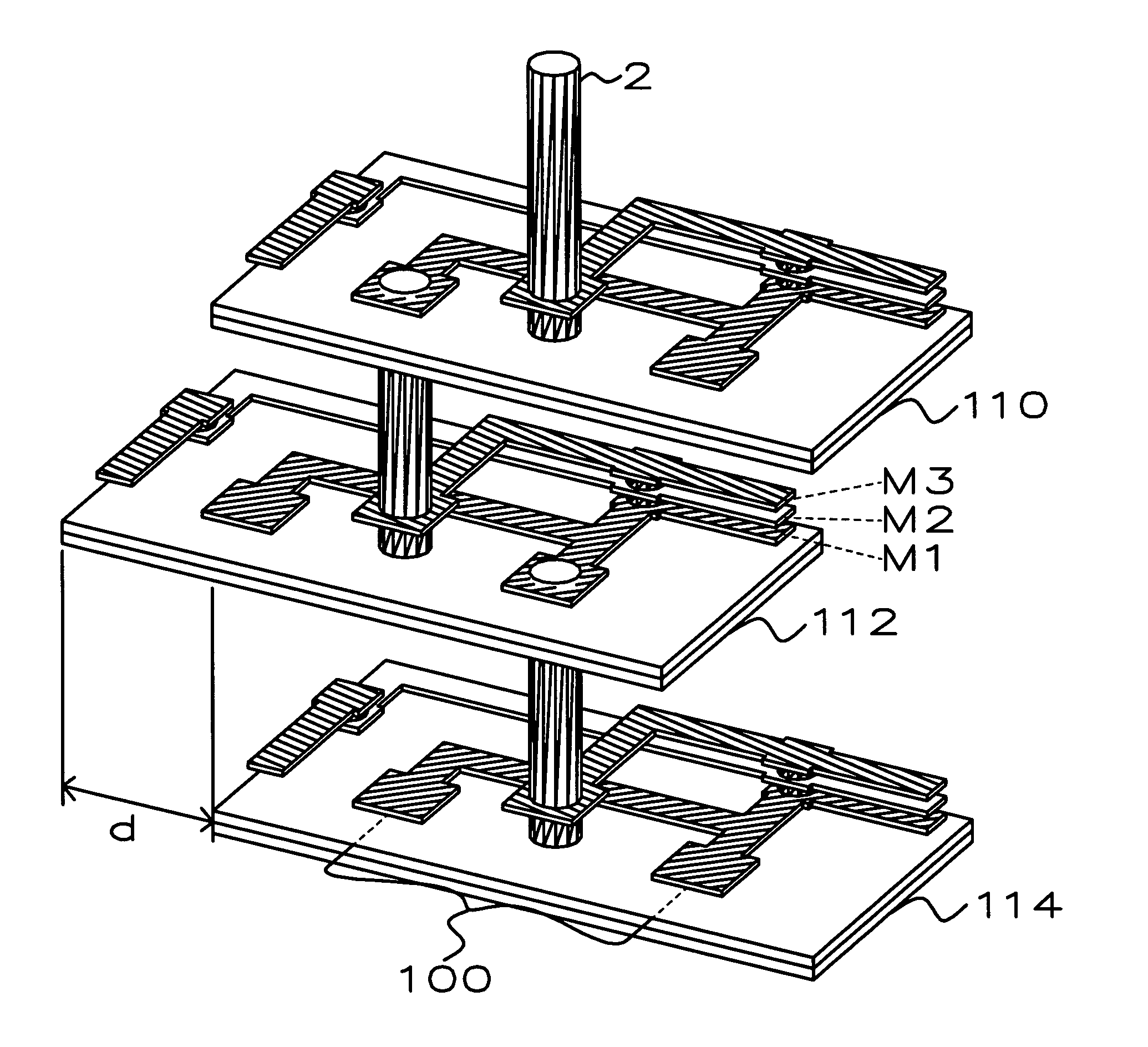
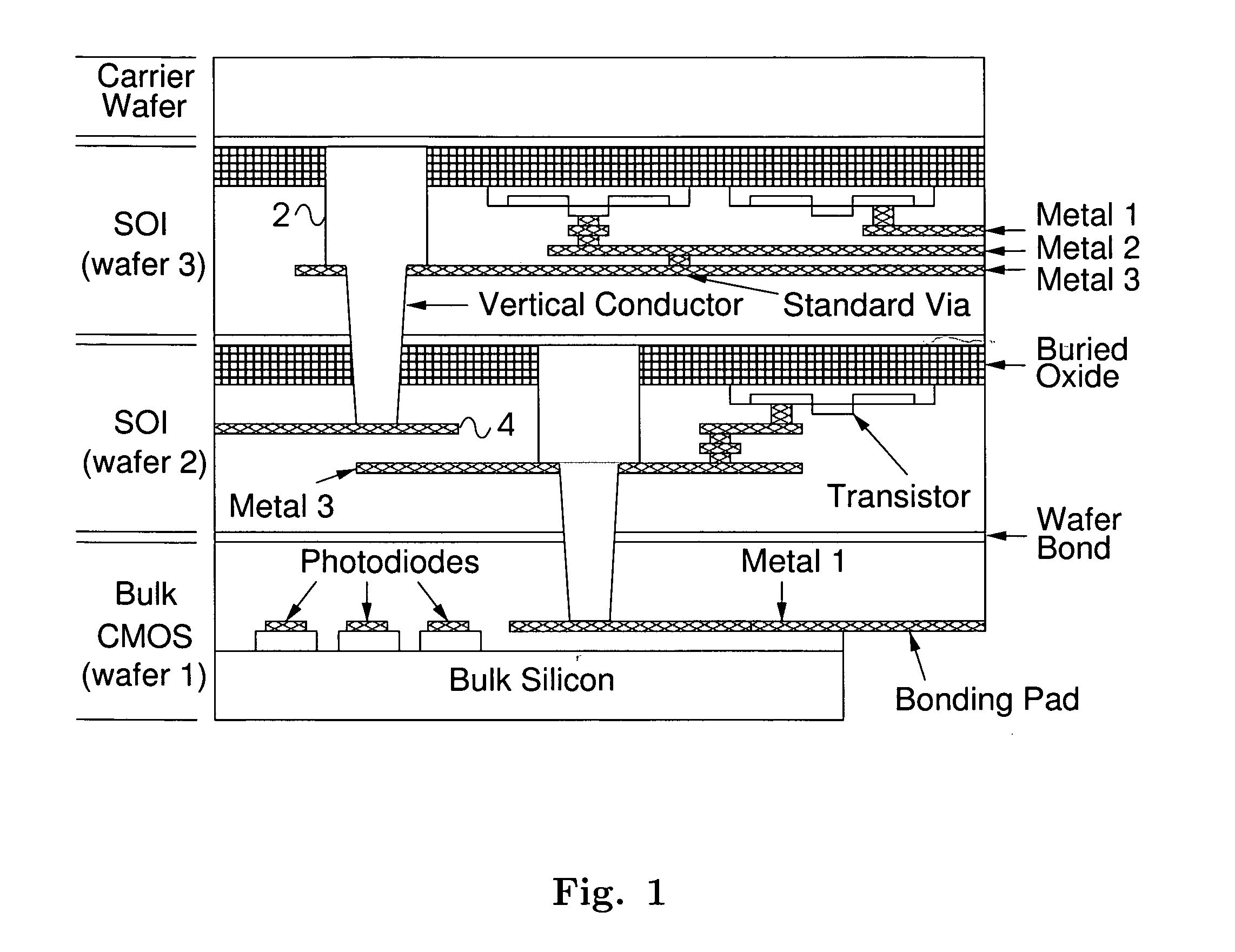
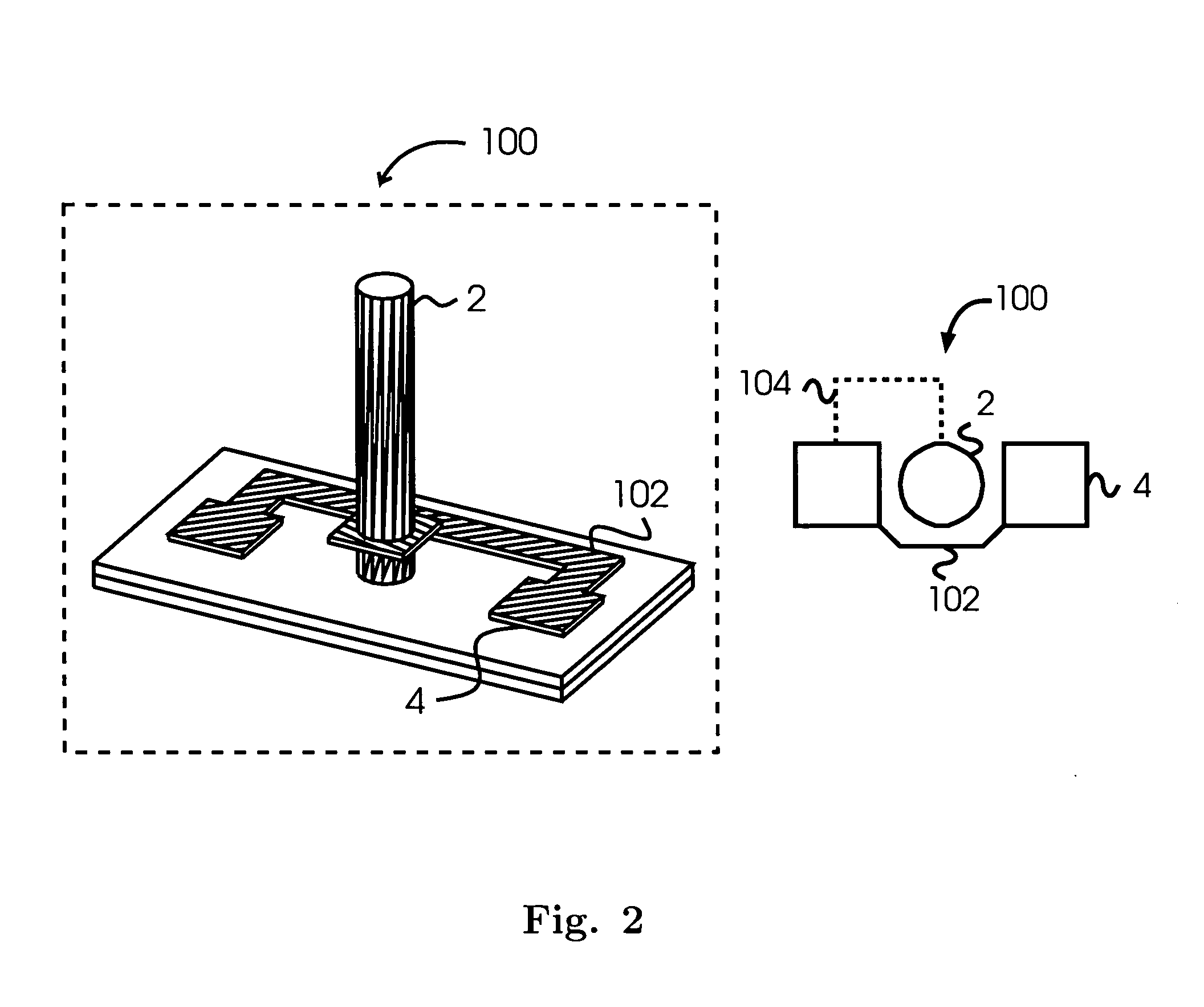
[0040]The present invention involves design techniques or methods that enable scalable integrated circuit systems. A single design and mask set is produced for one die, within a vertical three-dimensional stack of dies, and is reused for all dies with little or no design modification.

[0041]The system scales directly as the levels of stacking is increased while incurring no extra design effort as the stack height increases. Furthermore, the presented methods simplifies design verification since only a single layer of circuits needs to be verified instead of multiple layers.

[0042]Thus, the presented methods increase processing power, chip integration and data storage density in the same planar integrated circuit area with small additional design effort for the single design that is reused...


PUM


Abstract

The design methods described enable three-dimensional integrated circuit systems in which all of the dies, in a vertically bonded stack of dies, are identical. Only one mask set and wafer type is required since a single circuit design is produced for one die in the stack and reused for all the dies with little or no modification. The system scales directly as the level of stacking is increased while incurring no extra design effort, beyond that required for the initial design.

Description

[0001]This application claims priority from U.S. Application No. 60 / 365,807 file Mar. 21, 2002.FIELD OF THE INVENTION[0002]Scalable electronic circuit system composed of stacked layers of the same or similar circuitry.BACKGROUND OF THE INVENTION[0003]Traditionally integrated circuits have been built in a planar fashion, with a single layer of transistors. New developments in manufacturing process technology allow wafers to be vertically stacked and fine-grained vertical conductors formed between circuits on adjacent dies [1, 2, 3, 4, 5, 6, 7]; U.S. Pat. No. 5,627,106; U.S. Pat. No. 5,877,034; U.S. Pat. No. 5,998,808; U.S. Pat. No. 6,185,122; U.S. Pat. No. 6,034,882. Alternatively, layers of transistor circuits may be interconnected with coarser grain conductors such as coaxial lines, (C-4) solder pads, solder mounds, solder bumps, wire bounds, wire interconnects or embedded wiring as in U.S. Patent Application No. 20010033030; U.S. Patent Application No. 20010033509; U.S. Patent Aap...

Claims


Application Information

Patent Timeline
Patent Type & Authority Patents(United States)
IPC IPC(8): H05K1/11H01L23/52H01L23/535H01L25/065H05K3/46
CPCH01L25/0657H05K1/115H01L27/0688H01L27/1207H01L23/5226H01L2924/3011H01L2924/0002H05K3/4611H05K2201/09709H01L2225/06513H01L2225/06541H01L2225/06565H01L2225/06544H01L2924/00H05K1/11
Inventor SUNG, RAYMOND JIT-HUNGBRANDON, TYLER LEEKOOB, JOHN CONRADELLIOTT, DUNCAN GEORGELEDER, DANIEL ARIE
Owner SUNG RAYMOND JIT HUNG
Why Eureka
Try Eureka