

Resistor process
a resistor and process technology, applied in the direction of resistor details, resistor housing/enclosement/embedding, resistor incorporation, etc., can solve the problems of consuming valuable surface area of the panel, increasing the overall size of the assembly, and introducing significant unwanted capacitance or inductan
- Summary
- Abstract
- Description
- Claims
- Application Information
AI Technical Summary
Benefits of technology
Problems solved by technology
Method used
Image

Examples
Embodiment Construction
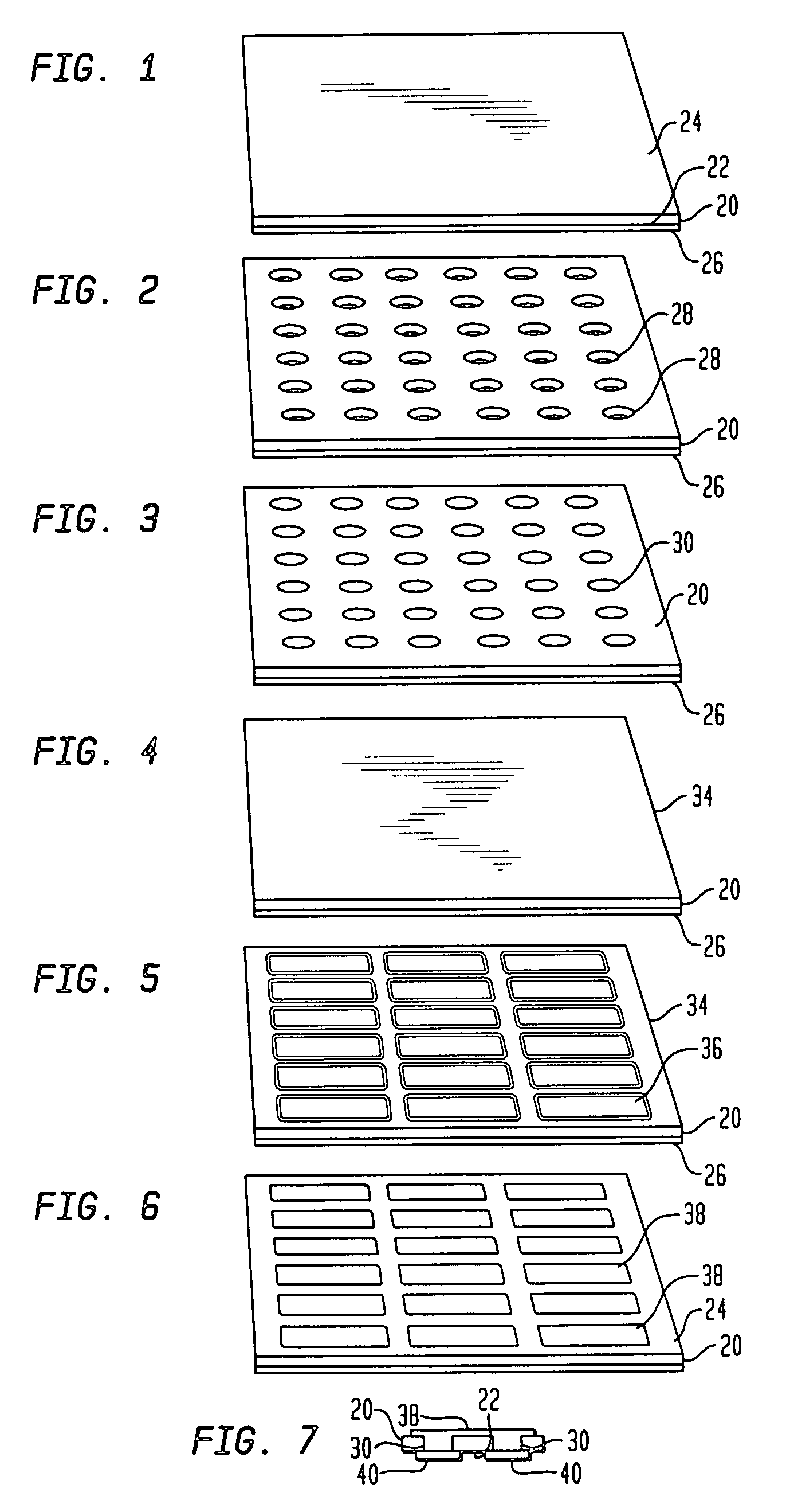
[0018]A process according to one embodiment of the invention, begins with a body in the form of a layer or sheet 20 of a polymeric dielectric material such as polyimide, or BT resin polymer having a bottom surface 22 and a top surface 24. The polymeric body typically has a thickness or dimension between its top and bottom surfaces on the order of 150 μm or less, most typically 100 μm or less and most commonly between about 25 and about 75 μm, and may be a dielectric layer of the type commonly employed in making flexible printed circuits or tape automated bonding (“TAB”) tapes. Other thicknesses and types of dielectric layers may be employed. Also, the dielectric layer may be formed from a photoimageable material. As used in this disclosure, the term “photoimageable material” refers to a material which can be exposed to radiant energy such as visible or ultraviolet light in a pattern and which will cure or degrade in only those portions of the material exposed to such energy so that ...
PUM
 Abstract
Description
Claims
Application Information