
Standard sample for transmission electron microscope (TEM) elemental mapping and TEM elemetal mapping method using the same

a technology of which is applied in the field of standard sample for transmission electron microscope and elemental mapping using the same, can solve the problems of reducing the spatial resolution power of mapping images and the microbeam analysis technique that has not been standardized

Active Publication Date: 2006-05-30
SAMSUNG ELECTRONICS CO LTD +2
View PDF2 Cites 8 Cited by
  • Summary
  • Abstract
  • Description
  • Claims
  • Application Information

AI Technical Summary

Problems solved by technology

However, the microbeam analysis technique has not been standardized, and also the manufacture, research, and development of standard samples for microbeam analysis are far behind a desirable level.
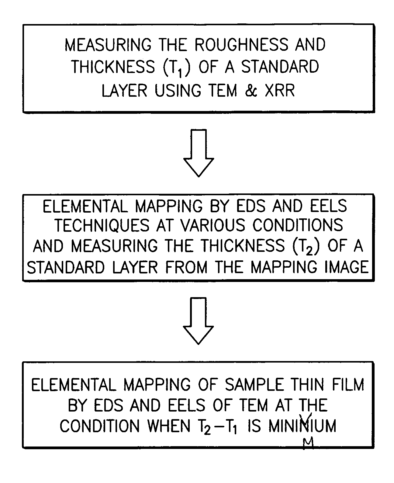
In principle, the use of the EDS mapping method results in a decrease in spatial resolution power of a mapping image since a characteristic X ray, which is generated when an impinging beam diffuses in a sample, is used.

Method used


Image

  • Standard sample for transmission electron microscope (TEM) elemental mapping and TEM elemetal mapping method using the same
  • Standard sample for transmission electron microscope (TEM) elemental mapping and TEM elemetal mapping method using the same
  • Standard sample for transmission electron microscope (TEM) elemental mapping and TEM elemetal mapping method using the same

Examples


example 1

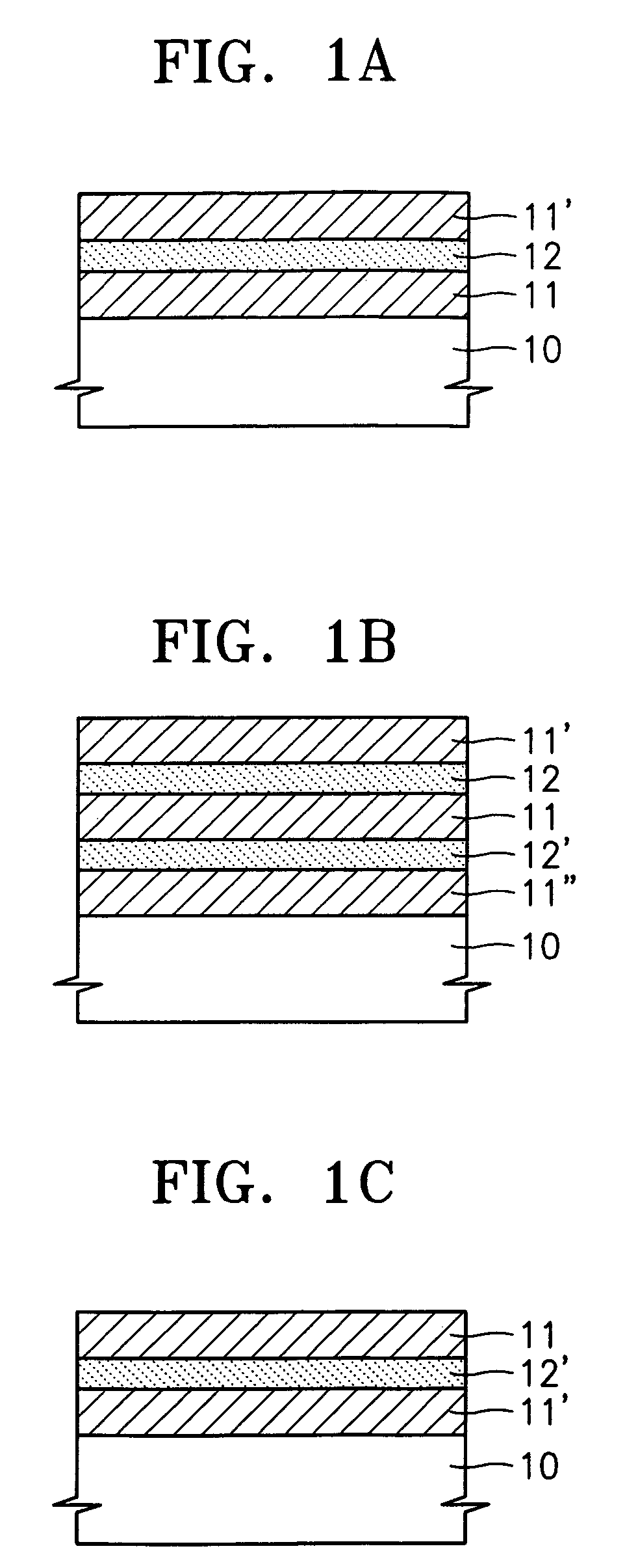
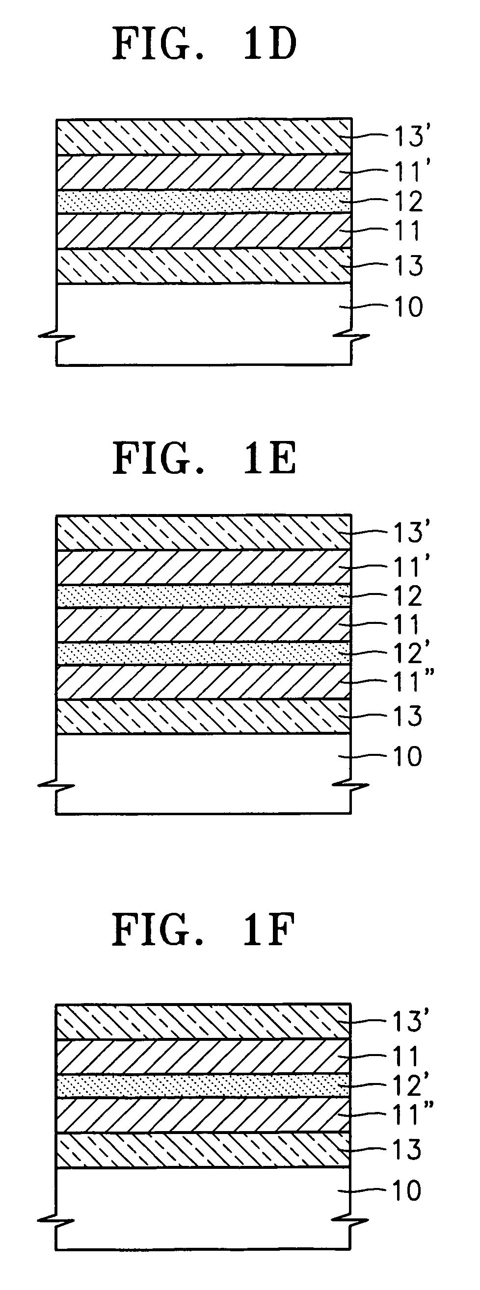
[0056]A multi-layered nanometer-sized thin film to be used as a standard sample was prepared by sequentially depositing a Ta film (thickness: 3 nm), a NiFe film (thickness: 3 nm), a MnPt film (thickness: 1.5 nm), a CoFe film (thickness: 2 nm), a Ru film (thickness: 0.8 nm), a CoFe film (thickness: 2.5 nm), an amorphous aluminium oxide film, a CoFe film (thickness: 2.5 nm), a NiFe film (thickness: 4 nm), and a Ta film (thickness: 5 nm) on a silicon substrate.

[0057]The standard sample was analysed using TEM, and the results are shown in FIG. 3.

[0058]FIG. 3 illustrates a zero loss image of the standard sample produced according to Example 1. Referring to FIG. 3, the measured thickness of the amorphous aluminium oxide film was about 1.2 nm.

[0059]The standard sample was analysed using 2-wavelength XRR, and the results are shown in FIG. 4.

[0060]Referring to FIG. 4, the measured thickness of the amorphous aluminium oxide film was about 1.0 nm.

[0061]The standard sample was analysed using ED...


PUM

PropertyMeasurementUnit
thicknessaaaaaaaaaa
thicknessaaaaaaaaaa
atomic numbersaaaaaaaaaa

Abstract

A standard sample for transmission electron microscopy (TEM) elemental mapping and a TEM elemental mapping method using the same are provided. The standard sample includes a substrate; a first crystalline thin film containing heavy atoms formed on the substrate; a first amorphous thin film having oxides or nitrides containing light atoms and having a thickness of 1–5 nm or 6–10 nm formed on the first crystalline thin film; a second crystalline thin film containing heavy atoms formed on the first amorphous thin film. The standard sample can be used to correct TEM, EDS and EELS mapping results of a multi-layered nanometer-sized thin film and to optimize mapping conditions.

Description

BACKGROUND OF THE INVENTION[0001]Priority is claimed to Korean Patent Application No. 10-2004-0003253, filed on Jan. 16, 2004, in the Korean Intellectual Property Office, the disclosure of which is incorporated herein in its entirety by reference.[0002]1. Field of the Invention[0003]The present invention relates to a standard sample for transmission electron microscope (TEM) elemental mapping and TEM elemental mapping using the same, and more particularly, to a standard sample for transmission electron microscope (TEM) elemental mapping which can be used to correct results of elemental mapping of nanometer-sized thin films, which are obtained by energy dispersive spectroscopy (EDS) and electron energy loss spectroscopy (EELS) methods using TEM, and to optimize mapping conditions, and TEM elemental mapping method using the same.[0004]2. Description of the Related Art[0005]Recently, industrialized countries have strategically intensified ISO international standardization activities to...

Claims


Application Information

Patent Timeline
Patent Type & Authority Patents(United States)
IPC IPC(8): G01N23/02H01J37/26G01N1/28G01N23/04G01N23/08G01N33/04
CPCG01N23/083H01J2237/2516E05B15/00
Inventor PARK, GYEONG-SUKAJI, KAZUTOSHIPARK, JONG-BONGTERADA, SHOHEIHIRANO, TATSUMISONG, SE-AHN
Owner SAMSUNG ELECTRONICS CO LTD
Learn More