Method for reading a nonvolatile memory device and nonvolatile memory device implementing the reading method

a nonvolatile memory and reading method technology, applied in the direction of digital storage, static storage, instruments, etc., can solve the problems of disadvantageous use of this type of sense amplifier, both sense amplifiers of parallel type and sense amplifiers of synchronous-serial-dichotomic type are very bulky

Inactive Publication Date: 2006-05-30
MICRON TECH INC
View PDF13 Cites 53 Cited by
  • Summary
  • Abstract
  • Description
  • Claims
  • Application Information

AI Technical Summary

Problems solved by technology

Although widely used, sense amplifiers of parallel type and sense amplifiers of synchronous-serial-dichotomic type have a number of drawbacks that do not enable an adequate exploitation of all their qualities.
First, both sense amplifiers of parallel type and sense amplifiers of synchronous-serial-dichotomic type are very bulky.
In fact, sense amplifiers of parallel type require a comparator stage for each of the bits stored in the memory cells, which, as is known, occupies a non-negligible area, so that the use of this type of sense amplifier becomes in effect disadvantageous as the number of bits stored in the memory cells increases.
In addition, this type of sense amplifier requires an accurate management of the various dichotomic steps so that the circuit complexity of the control stage, and hence its bulk, increases significantly as the number of bits stored in the memory cells increases.
For the above reasons, the reading speed of synchronous-serial-dichotomic sense amplifiers is not very high; in particular, the total time for reading the contents of a nonvolatile memory cell has on average, in this type of sense amplifier, rather high values of the order of 20–25 ns, which, in some applications, is not acceptable.
Notwithstanding the considerable improvements achieved, reading of multilevel memory cells continues in any case in general to be afflicted by a series of problems linked essentially to the intrinsic characteristics of the memory device in general and of the memory cells in particular.
In particular, it has been verified that in multilevel memory cells the outcome of reading a datum stored in a block of memory cells belonging to a same sector may also depend, to a non-negligible extent, upon the datum itself; i.e., the reading of the contents of a given memory cell is influenced by the reading of the contents of the adjacent memory cells, and this influence is particularly significant in multilevel memory cells, so much so as possibly to lead to reading errors.
With this architecture, the voltage on the common node connected to the source terminals of all the memory cells belonging to a same sector depends upon the current drained by the memory cells being read, so that, given that the outcome of the reading of the contents of a memory cell depends to a significant extent upon the voltage present on its own source terminal, the variation that the voltage present on the common node can undergo according to the datum that is being read may lead to errors in reading the contents of a memory cell.
A further problem is linked to the way the references necessary for reading are generated.
This solution, albeit with the minor generation errors, entails, however, the use of current mirrors made up of transistors of rather large size, so that this solution has the biggest bulk and a current consumption proportional to the size of the transistors for charging the capacitances associated to their gate regions.
This solution, albeit having a smaller bulk in so far as it does not entail current-mirror transistors, leads, however, during testing of the memory device, to long times for checking the references generated.
A further problem that adversely affects reading of multilevel memory cells is represented by the so-called “bending” of the voltage-current characteristics of the memory cells, this bending being in turn originated by the so-called “column path” created by the current of the memory cells being read.
In particular, in FIG. 8, a dashed line illustrates the ideal voltage-current characteristic of a memory cell, while a solid line illustrates the actual voltage-current characteristic of a memory cell, which has an evident bending downwards for high cell currents, being caused by the voltage drops on the column-selection transistors and possibly leading to an evident adverse effect on reading.

Method used


Image

  • Method for reading a nonvolatile memory device and nonvolatile memory device implementing the reading method
  • Method for reading a nonvolatile memory device and nonvolatile memory device implementing the reading method
  • Method for reading a nonvolatile memory device and nonvolatile memory device implementing the reading method

Examples


Embodiment Construction

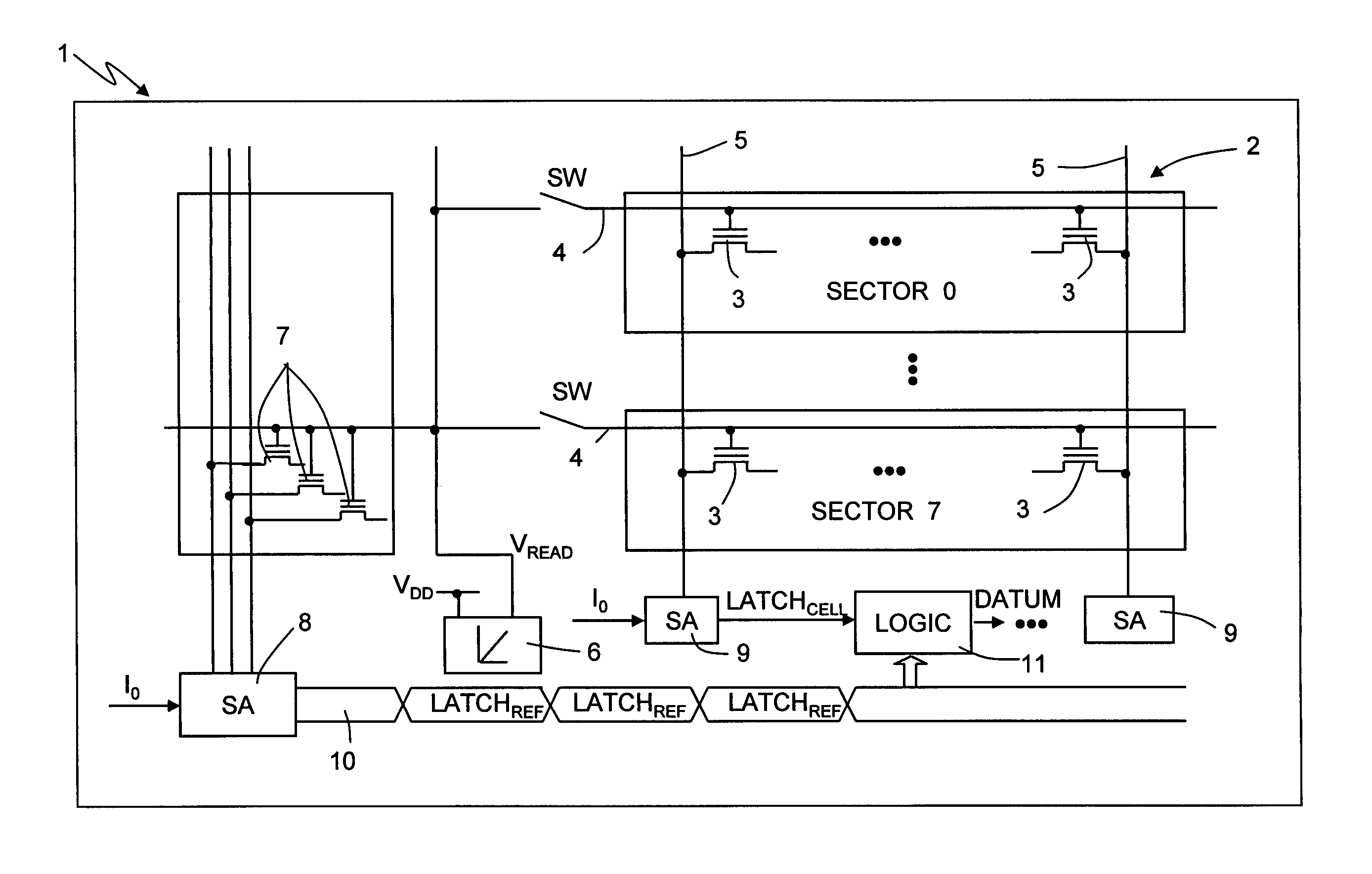
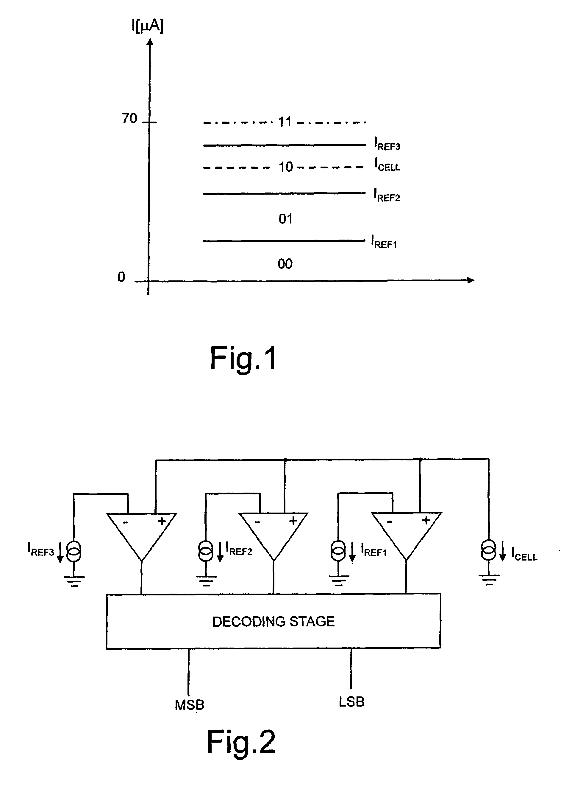
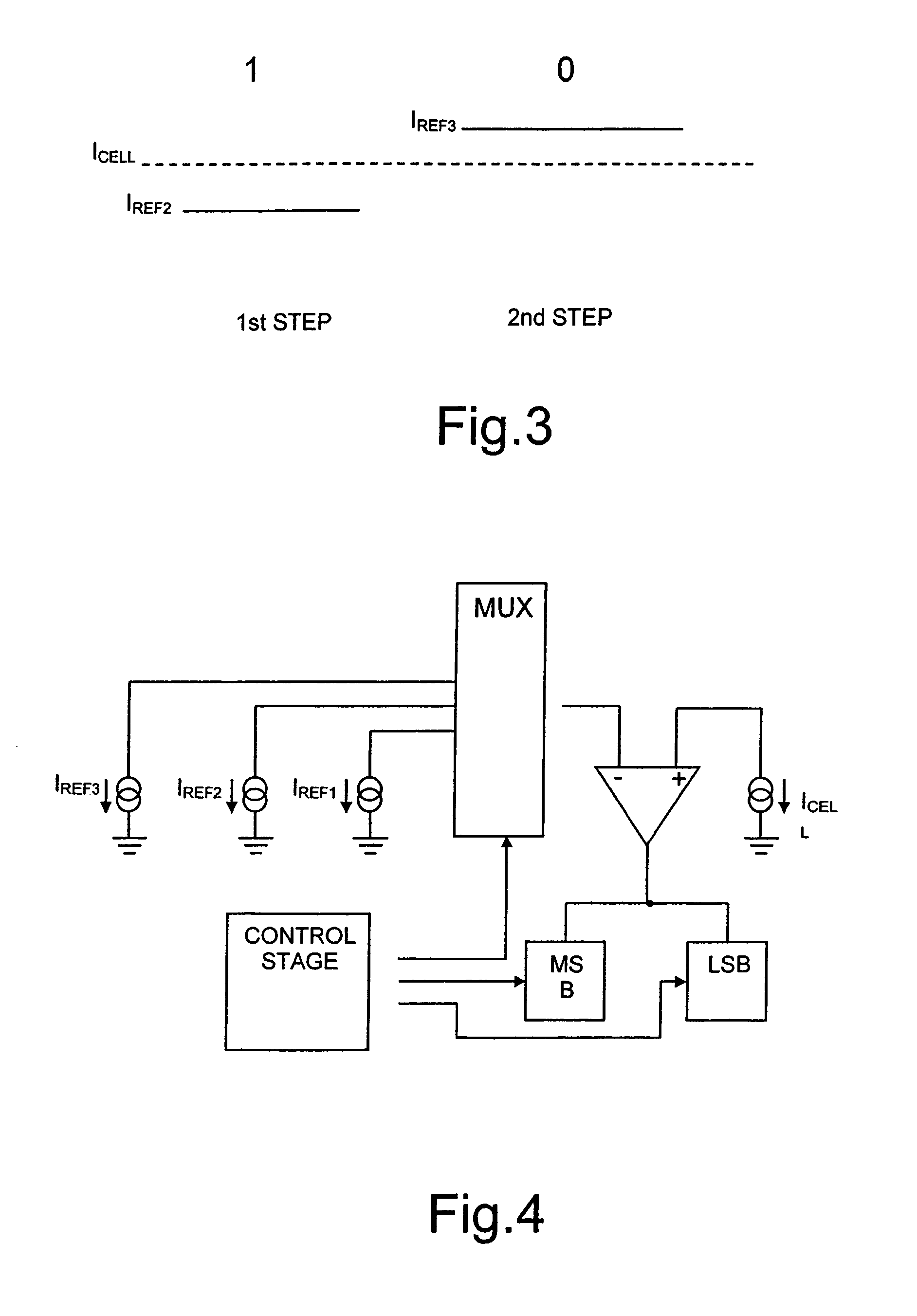
[0084]Only in order to facilitate understanding, the present invention will be described hereinafter with reference to the reading the contents of multilevel memory cells which store two bits, i.e., memory cells in which the threshold voltage can assume four distinct levels, where, as described previously, the current of the array memory cell ICELL that it is intended to read is compared with three different reference currents IREF1, IREF2, IREF3, which are generated by three distinct reference memory cells having three distinct threshold voltages.

[0085]Each time it will be indicated how what is described with regard to the specific example can be applied to memory cells to be read which store n bits, i.e., memory cells in which the threshold voltage can assume 2n distinct values.

[0086]One innovative idea that underlies the present invention is that of:[0087]biasing the array memory cell and the three reference memory cells so as to modify their respective current-conduction states ...


PUM


Abstract

A reading method for a nonvolatile memory device, wherein the gate terminals of the array memory cell and of the reference memory cell are supplied with a same reading voltage having a ramp-like pattern, so as to modify their current-conduction states in successive times, and the contents of the array memory cell are determined on the basis of the modification order of the current-conduction states of the array memory cell and of the reference memory cell.

Description

BACKGROUND OF THE INVENTION[0001]1. Field of the Invention[0002]The present invention relates to a method for reading a nonvolatile memory device and to a nonvolatile memory device implementing the reading method.[0003]2. Discussion of the Related Art[0004]As is known, in nonvolatile memory cells of the floating-gate type, a logic state is stored by programming the threshold voltage of the memory cells through the definition of the amount of electrical charge stored in the floating-gate region.[0005]Thanks to the evolution of technological processes, allowing the implementation of elementary memory devices of increasingly smaller size, in the last few years semiconductor memory devices having very high memory capacities have been obtained. A further increase in the memory capacity has been obtained by resorting to multilevel storage, which enables an increase in the memory density for the same technological generation. In fact, with this technique, more information bits are stored w...

Claims


Application Information

Patent Timeline
Patent Type & Authority Patents(United States)
IPC IPC(8): G11C16/04G11C16/06G11C11/56
CPCG11C11/5642G11C2211/5634G11C16/32
Inventor VIMERCATI, DANIELE
Owner MICRON TECH INC
Why Eureka
Try Eureka