Semiconductor memory storage device capable of high operating speed

Inactive Publication Date: 2006-05-30
PANASONIC CORP
View PDF9 Cites 6 Cited by
  • Summary
  • Abstract
  • Description
  • Claims
  • Application Information

AI Technical Summary

Benefits of technology

[0034]In still another preferred aspect of the configuration described above, the memory cell array further comprises a metal wire arranged adjacently in parallel to the dummy bit line and having an end thereof grounded, and a plurality of selective switching elements inserted at predetermined intervals on the metal wire. In this case, a parasitic capacitance is formed between the dummy bit line and the metal wire. By turning on/off the selective switching elements, the effective parasitic capacitance can be regulated. As a result, the proper timing of the enable signal for the sense amplifier can be easily achieved by regulating the discharge rate of the dummy bit line.
[0035]Also, in the configuration described above, each n-channel field-effect transistor may be replaced with an inverter for logically inverting outputs of the word line driver and a p-channel field-effect transistor with the gate thereof connected to the inverter and the source thereof connected to the high-potential side of the power supply. In this way, the discharge rate of the dummy bit line can be increased by increasing the gate voltage of the replica n-channel field-effect transistors to the source voltage. Also, an operation margin can be secured to compensate for a possible source voltage drop, thereby stabilizing the circuit operation.
[0036]According to yet another aspect of the invention, the configuration described above preferably further comprises a row decoding circuit for stopping the operation of selecting a selected word line driver in response to the enable signal for the sense amplifier. As a result, the word line thus far selected is deactivated by the enable signal of the sense amplifier, and therefore the activation time of the word lines is reduced to a required minimum thereby reducing the power consumption.
[0037]According to a further aspect of the inventio

Problems solved by technology

Since these two signal lines are separate from each other, the accuracy of the timing at which the word line is actually activated is low.
Also, the use of a replica memory cell having a similar conf

Method used


Image

  • Semiconductor memory storage device capable of high operating speed
  • Semiconductor memory storage device capable of high operating speed
  • Semiconductor memory storage device capable of high operating speed

Examples


Example

FIRST EMBODIMENT

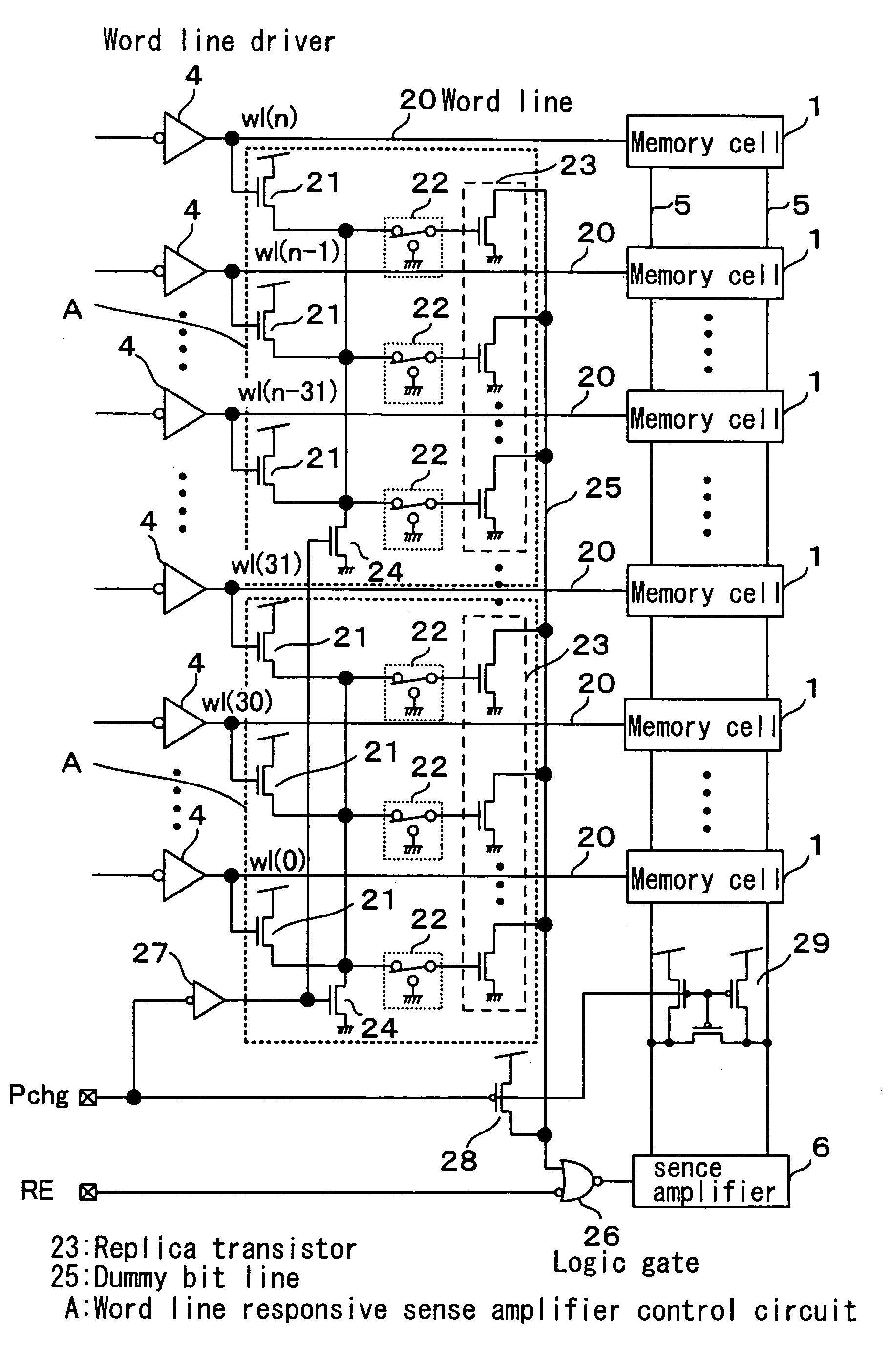
[0049]FIG. 1 is a schematic circuit diagram of a static random-access memory (hereinafter referred to as SRAM) as a semiconductor memory storage according to a first embodiment of the invention. In FIG. 1, the same component parts as the corresponding ones in FIG. 5 showing a conventional semiconductor memory storage are designated by the same reference numerals, respectively and not described again. In FIG. 1, each of a plurality of word lines 20 connected to the corresponding one of a plurality of word drivers 4 and the corresponding one of a plurality of memory cells 1 branches and is connected to the gate of the corresponding one of a plurality of n-channel field-effect transistors (hereinafter referred to as the n-ch transistors) 21 as a word line responsive switching element. The drain of the n-ch transistor 21 is connected to the high potential side of a power supply, and the source thereof is connected through a selective switching element 22 to the gate of a...

Example

SECOND EMBODIMENT

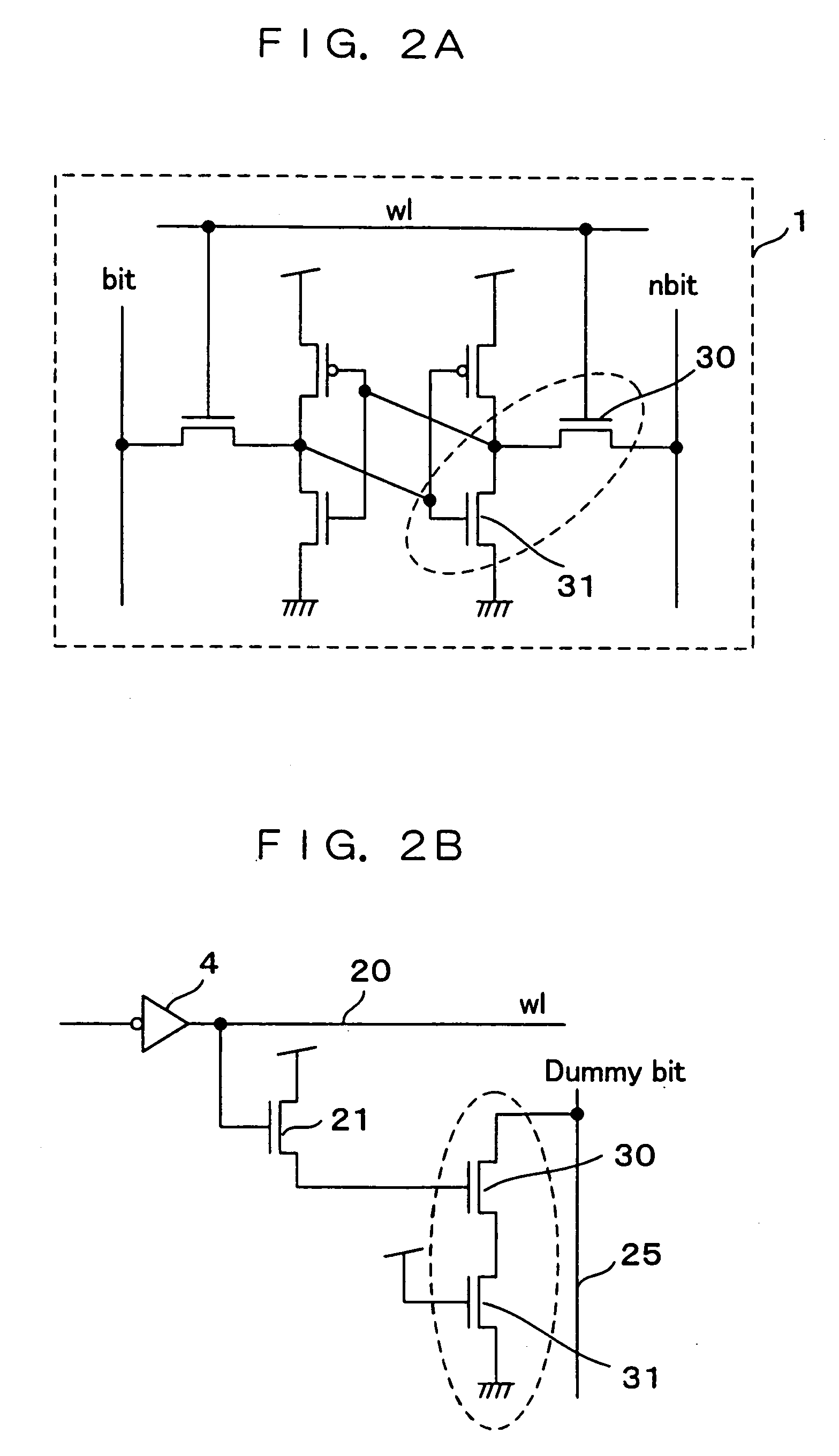
[0056]FIG. 2A is a schematic circuit diagram of a SRAM as a semiconductor memory storage according to a second embodiment of the invention. In FIG. 2A, the same component parts as the corresponding ones of the prior art shown in FIG. 5 and the embodiment shown in FIG. 1 are designated by the same reference numerals, respectively, and not described again. In FIG. 2, the replica transistor 23 shown in FIG. 1 is arranged as a dummy cell for optical correction. The dummy cell for optical correction is arranged in order to suppress the variations of the characteristics of the memory cells.

[0057]The pass transistor 30 and the drive transistor 31 shown in FIG. 2A are used as dummy transistors for optical correction. The replica transistor 23 in FIG. 1 is configured of a pass transistor 30 shown in FIG. 2B and a drive transistor 31 with the gate thereof fixed to the high potential side of the power supply in saturated form.

[0058]The operation of the semiconductor memory sto...

Example

THIRD EMBODIMENT

[0060]FIG. 3 is a schematic circuit diagram of a SRAM as a semiconductor memory storage according to a third embodiment of the invention. In FIG. 3, the same component parts as the corresponding ones of the prior art shown in FIG. 5 and the embodiment shown in FIG. 1 are designated by the same reference numerals, respectively, and therefore not described again. In FIG. 3, a logically inverting gate (inverter) 40 is connected to the branch line from each word line 20 on the output side of each word line driver 4, and the output of the logically inverting gate 40 is connected to the gate of a p-channel field-effect transistor (hereinafter referred to as the p-ch transistor) 41 as a work line responsive switching element. The source of the p-ch transistor 41 is connected to the high potential side of the power supply. The drain of the p-ch transistor 41 is connected to the gate of the replica transistor 23. The drain of each p-ch transistor 41, on the other hand, is con...


PUM


Abstract

A semiconductor memory storage is disclosed, in which the gate of each of a plurality of n-channel transistors is connected to the corresponding one of a plurality of word lines on the output side of each word line driver. The source of the n-channel transistor is connected through a selective switching element to the gate of the corresponding one of a plurality of replica transistors connected to a dummy bit line. The gate of each replica transistor is connected to the corresponding one of discharge transistors. The dummy bit line is connected to a sense amplifier through a logic gate.

Description

BACKGROUND OF THE INVENTION[0001]The present invention relates to a semiconductor memory storage, and in particular to a random-access semiconductor memory storage comprising a memory cell array having a plurality of memory cells arranged in a matrix, a plurality of word line drivers each connected through the corresponding one of a plurality of word lines to the corresponding one of a plurality of the memory cells arranged in a row in the memory cell array for activating a selected word line as the result of decoding an address signal, and a sense amplifier for detecting the activated state of the memory cells.[0002]A semiconductor memory storage is known which has a circuit for correcting the effect of variations in production conditions for forming a memory cell array on a silicon substrate, and variations of the environmental temperature conditions and voltage conditions.[0003]FIG. 5 is a circuit diagram schematically showing the conventional semiconductor memory storage. This s...

Claims


Application Information

Patent Timeline
IPC IPC(8): G11C7/00G11C11/419G11C7/06G11C7/12G11C7/14
CPCG11C7/06G11C7/14G11C7/12G11C2207/065
Inventor TSUJIMURA, KAZUKIKANEHARA, HIDENARISUMITANI, NORIHIKO
Owner PANASONIC CORP
Why Eureka
Try Eureka