Phase-Locked Loop
a phase lock and loop technology, applied in the direction of phase difference detection, automatic control of pulses, electrical devices, etc., can solve the problems of insufficiently broad lock range, lock cannot be held, and lock range would be extremely reduced, so as to achieve the effect of enlarge the lock rang
- Summary
- Abstract
- Description
- Claims
- Application Information
AI Technical Summary
Benefits of technology
Problems solved by technology
Method used
Image
Examples
first embodiment
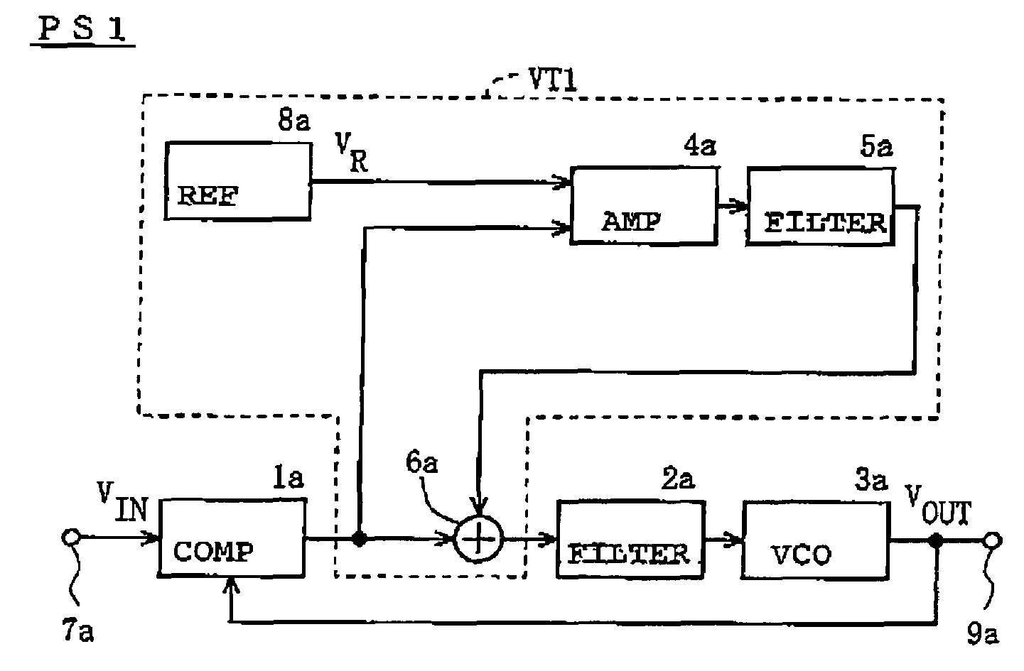
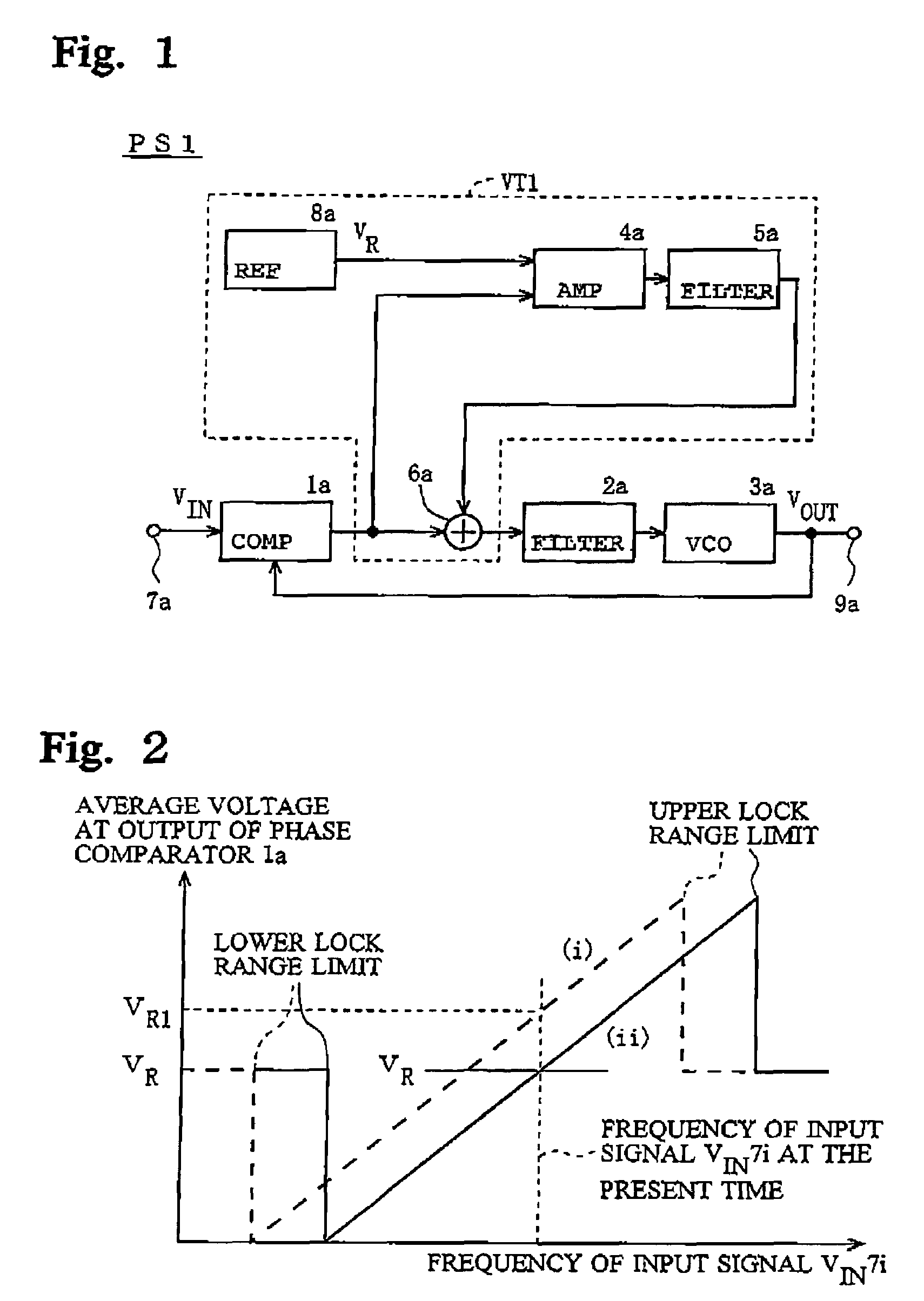
[0065]FIG. 1 is a block diagram showing a phase lock circuit(phase-locked loop circuit) PS1 that is the present invention in.
[0066]The phase lock circuit PS1 has a phase comparator 1a, a loop filter 2a, a voltage control oscillator(voltage-controlled oscillator) 3a, a signal input terminal 7a, a signal output terminal 9a and a voltage tracking circuit VT1 that is an additional loop. The phase comparator 1a, loop filter 2a and voltage control oscillator 3a defines the main body of a phase lock circuit. The voltage tracking circuit VT1 comprises a reference voltage generator 8a, a differential amplifier 4a, a filter 5a and an adder 6a. The phase comparator 1a will be described to be EXOR so long as it is not particularly declined below.
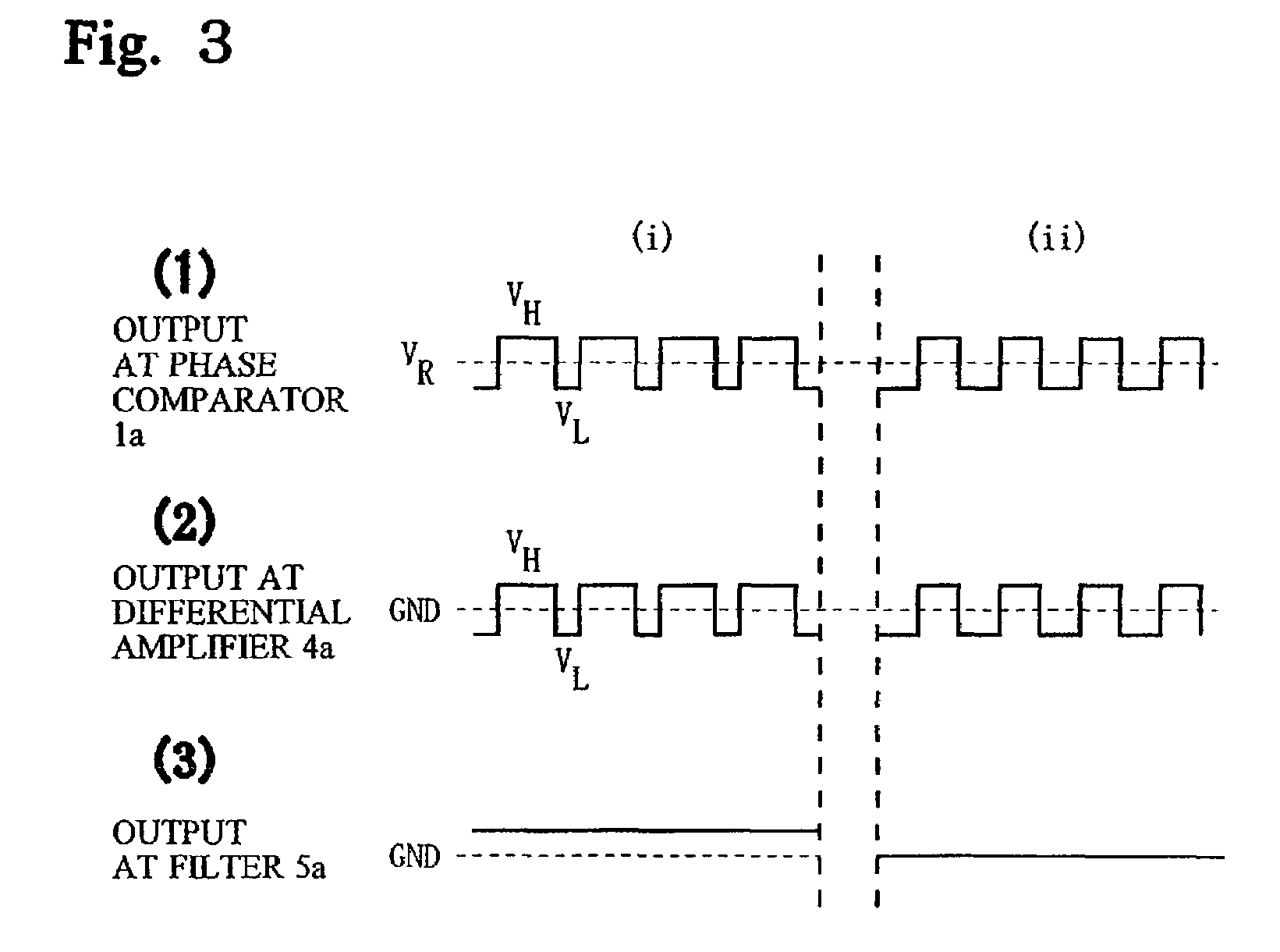
[0067]The differential amplifier 4a outputs a voltage proportional to a difference between the output voltage of the phase comparator 1a and the output voltage VR of the reference voltage generator 8a. The filter 5a converts the output voltage of the di...
second embodiment
[0088]FIG. 4 is a block diagram showing a phase lock circuit PS2 that is the present invention.
[0089]The phase lock circuit PS2 comprises a phase comparator 1b, a loop filter 2b, a voltage control oscillator 3b, a signal input terminal 7b, a signal output terminal 9b, and a voltage tracking circuit VT2. The voltage tracking circuit VT2 comprises a reference voltage generator 8b, a differential amplifier 4b, a filter 5b and an adder 6b.
[0090]The phase lock circuit PS2 is basically the same as the phase lock circuit PS1, except that the output voltage of the filter 5b is added to the output voltage of the loop filter 2b rather than to the output voltage of the phase comparator 1b.
[0091]Operation and advantage in the phase lock circuit PS2 are substantially the same as those of the phase lock circuit PS1.
third embodiment
[0092]FIG. 5 is a block diagram showing a phase lock circuit PS3 that is the present invention.
[0093]The phase lock circuit PS3 has a phase comparator 1c, a loop filter 2c, a voltage control oscillator 3c, a signal input terminal 7c, a signal output terminal 9c and a voltage tracking circuit VT3. The voltage tracking circuit VT3 comprises a reference voltage generator 8c, a differential amplifier 4c, a first filter 10c, a second filter 5c and an adder 6c.
[0094]FIG. 6 is a view showing signal waveforms in the primary parts of the phase lock circuit PS3.
[0095]FIG. 6(i) is a view showing the operation of the phase lock circuit immediately after it has been shifted from its unlocked state to its locked state while FIG. 6 (ii) shows such a sate that the duty ratio in the output of the phase comparator 1c is maintained constant (about 50% in FIG. 6) by the voltage tracking circuit VT3.
[0096]The operational principle and advantage of the phase lock circuit PS3 are substantially the same a...
PUM
 Abstract
Description
Claims
Application Information


